Trench-type super junction manufacturing method

A manufacturing method and super-junction technology, applied in semiconductor/solid-state device manufacturing, electrical components, circuits, etc., can solve problems affecting production yield, device failure, and device reverse leakage current increase

Active Publication Date: 2018-08-21
SHANGHAI HUAHONG GRACE SEMICON MFG CORP
View PDF4 Cites 0 Cited by
  • Summary
  • Abstract
  • Description
  • Claims
  • Application Information

AI Technical Summary

Problems solved by technology

The biggest difficulty of this process is to fill the trench with silicon epitaxy. The existing manufacturing method is very easy to cause a sharp increase in the reverse leakage current of the device, which will lead to the failure of the device and seriously affect the production yield.

Method used


Image

  • Trench-type super junction manufacturing method
  • Trench-type super junction manufacturing method
  • Trench-type super junction manufacturing method

Examples


Embodiment Construction

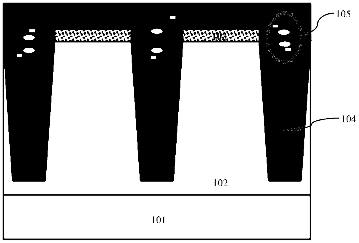
[0037] First introduce the problems of the existing trench superjunction manufacturing method, the present invention has made specific improvements to these technical problems, such as figure 1 Shown is a schematic structural diagram of a super junction formed by an existing trench-type super junction manufacturing method; the existing method includes the following steps:

[0038] Step 1: Provide a semiconductor substrate such as a silicon substrate 101 , and an N-type epitaxial layer such as an N-type silicon epitaxial layer 102 is formed on the surface of the semiconductor substrate 101 .

[0039] Step 2: Forming a plurality of trenches in the N-type epitaxial layer 102 by photolithography. The hard mask layer 103 is used when etching the trench.

[0040] Step 3: filling the trench with a P-type epitaxial layer such as a P-type silicon epitaxial layer 104 during epitaxial growth, and the P-type epitaxial layer 104 will simultaneously extend to the surface of the N-type epit...


PUM


Abstract

The invention discloses a manufacturing method for a groove type super junction. The method comprises the following steps of step 1 providing a semiconductor substrate whose surface is provided with a first conduction type epitaxial layer; step 2 forming a plurality of grooves in the first conduction type epitaxial layer; step 3 filling the grooves with a second conduction type epitaxial layer; step 4 carrying out a first chemical mechanical polishing process to remove the second conduction type epitaxial layer outside the grooves; and step 5 adopting a second epitaxial layer back etching process to carry out back etching on the first conduction type epitaxial layer and the second conduction type epitaxial layer to a certain depth simultaneously in order to remove cavities formed at the tops of the grooves and the lattice imperfection of the epitaxial layers. According to the method, the integrity of a lattice structure of the super junction can be improved, the method is convenient for manufacturing a high-performance super junction device, the reverse leakage current of the super junction device is reduced, and the yield rate of the super junction device is improved.

Description

technical field [0001] The invention relates to a manufacturing process method of a semiconductor integrated circuit, in particular to a manufacturing method of a trench type super junction. Background technique [0002] The super junction is composed of alternately arranged P-type thin layers and N-type thin layers formed in the semiconductor substrate. The existing super junction manufacturing method includes the manufacturing method of the trench type super junction. This method is through the trench To manufacture a super junction device, it is necessary to etch a trench with a certain depth and width on the N-type doped epitaxial layer on the surface of a semiconductor substrate such as a silicon substrate, and then use the method of epitaxial filling (ERI Filling) to fill the etched trench. The groove is filled with P-type doped silicon epitaxy, and the filled region is required to have a complete crystal structure so that high-performance devices can be fabricated in ...

Claims


Application Information

Patent Timeline
Patent Type & Authority Patents(China)
IPC IPC(8): H01L21/336H01L21/02
CPCH01L21/02H01L21/02104H01L21/02612H01L29/66409
Inventor 李昊
Owner SHANGHAI HUAHONG GRACE SEMICON MFG CORP
Why Eureka
Try Eureka