Thin film transistor sensor and fabrication method thereof
A technology of thin-film transistors and sensors, applied in the field of thin-film transistor sensors and their preparation, can solve problems such as difficult, difficult to achieve medical implantation in vivo, difficult to achieve biocompatibility, etc.
- Summary
- Abstract
- Description
- Claims
- Application Information
AI Technical Summary
Problems solved by technology
Method used
Image

Examples
preparation example Construction
[0030] At least one embodiment of the present invention provides a method for preparing a thin film transistor sensor, the method comprising the following steps:
[0031] forming a first gate on the inner side of the first flexible substrate to prepare a first substrate;
[0032] forming a second grid on the inner side of the second flexible substrate to prepare a second substrate;
[0033] An active layer facing the first gate and a source and a drain electrically connected to the active layer are also formed on the first flexible substrate;
[0034] The first substrate and the second substrate are disposed opposite to each other, so that the second gate and the first gate at least partly face each other and are insulated from each other when the TFT sensor is in a non-working state.
[0035] The preparation method of the thin film transistor sensor can adopt a common process, is simple and easy, and has low manufacturing and maintenance costs.
Embodiment 1
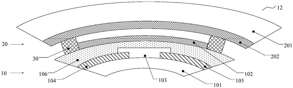
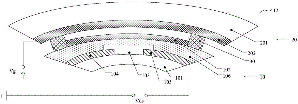
[0038] This embodiment provides a thin film transistor sensor 12, such as figure 2As shown, a first substrate 10 and a second substrate 20 disposed opposite to each other are included. The first substrate 10 includes a first flexible substrate substrate 101 and a first gate 102 disposed on the inner side of the first flexible substrate substrate 101 . The second substrate 20 includes a second flexible substrate substrate 201 and a second gate 202 disposed on the inner side of the second flexible substrate substrate 201 . The second gate 202 is at least partially opposite to the first gate 201 and is insulated from each other when the TFT sensor 12 is in a non-working state. An active layer 103 opposite to the first gate, and a source 104 and a drain 105 electrically connected to the active layer 103 are also disposed on the first flexible substrate 101 . The second gate 202 and the first gate 201 at least partly face each other so that the thin film transistor sensor 12 can...
Embodiment 2
[0055]Different from Embodiment 1, the thin film transistor sensor provided in this embodiment does not insulate the thin film transistor sensors 12 from each other when they are in a non-working state by disposing spacers around the edge of the first gate. but as Figure 7 As shown, a pressure conductive material 40 is provided between the first substrate 10 and the second substrate 20, thereby separating the first grid 102 from the second grid 202, and the pressure conductive material 40 is applied with a pressure equal to or exceeding a predetermined pressure. When conductive. The predetermined pressure may, for example, refer to the pressure at which the pressure conductive material changes from an insulating state to a conductive state. The pressure conductive material is in an insulating state when it is not under pressure or the pressure does not exceed a predetermined pressure, so that the first grid 102 and the second grid 202 are insulated from each other, and the p...
PUM
| Property | Measurement | Unit |
|---|---|---|
| thickness | aaaaa | aaaaa |
| thickness | aaaaa | aaaaa |
Abstract
Description
Claims
Application Information
 - R&D
- Intellectual Property
- Life Sciences
- Materials
- Tech Scout
- Unparalleled Data Quality
- Higher Quality Content
- 60% Fewer Hallucinations
Browse by: Latest US Patents, China's latest patents, Technical Efficacy Thesaurus, Application Domain, Technology Topic, Popular Technical Reports.
© 2025 PatSnap. All rights reserved.Legal|Privacy policy|Modern Slavery Act Transparency Statement|Sitemap|About US| Contact US: help@patsnap.com