Micron LED array based visible light communication system and construction method thereof

A technology of LED array and visible light communication, applied in short-range systems, free space transmission and other directions, can solve the problems of limiting the communication distance and practicability of micron LEDs, small output optical power of micron LEDs, and limiting communication speed, etc., and achieves strong practicality. high communication speed, high photoelectric modulation bandwidth effect

Active Publication Date: 2016-08-24
FUDAN UNIV
View PDF3 Cites 13 Cited by
  • Summary
  • Abstract
  • Description
  • Claims
  • Application Information

AI Technical Summary

Problems solved by technology

[0004] The modulation bandwidth of commercial LEDs commonly used in visible light communication is 5MHz to 20MHz, which limits the communication speed of LEDs; the modulation bandwidth of micron LEDs can reach more than 100MHz, but the output optical power of micron LEDs is relatively small, which limits the communication distance and Practicality

Method used


Image

  • Micron LED array based visible light communication system and construction method thereof
  • Micron LED array based visible light communication system and construction method thereof

Examples


Embodiment Construction

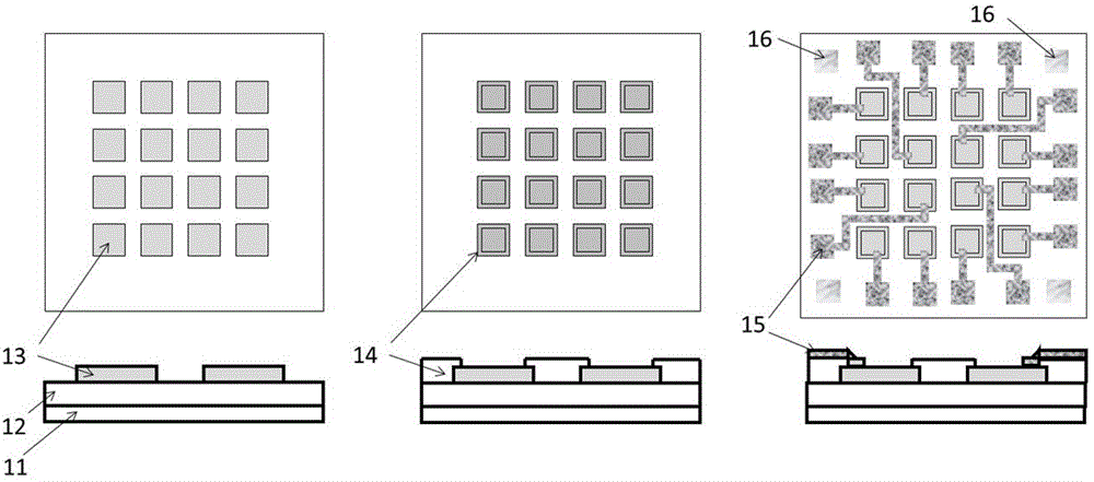
[0032] Preferred embodiments of the present invention will be described in detail below in conjunction with the accompanying drawings, so that the advantages and features of the present invention can be more easily understood by those skilled in the art. The present invention will be further described below in conjunction with the examples, but the present invention is not limited to the following examples.

[0033] (a) Fabrication of micro-LED arrays, figure 1 The upper figure in the schematic diagram is a top view, and the lower figure is a section view:

[0034] like figure 1 As shown, the GaN-based LED epitaxial layer is grown on the c-surface of the sapphire substrate, the p-type ohmic contact electrode Ni / Au (10nm / 25nm) is deposited, and the Ni / Au and a part of the GaN epitaxial layer are respectively etched away by reactive ion etching. The epitaxial layer is etched to a depth of 1 μm to expose the n-GaN 12, forming a micro-LED array mesa 13 with a length and width of...


PUM


Abstract

The invention belongs to the technical field of wireless communication, and specifically discloses a micron LED array based visible light communication system and a construction method thereof. The method comprises the following steps: etching through reactive ions to obtain a p type micron LED mesa array, wherein a size of a mesa is less than 100 microns; depositing an insulated passivation layer; forming holes in the insulated layer under an area where electrodes are to be constructed; preparing p type and n type electrodes to control each LED unit of a micron LED array; integrating the micron LED array and an optical collimating lens; integrating a receiving end high-speed photoelectric detector and a focusing lens through an OFDM modulation technology so as to achieve line-of-sight communication and non-line-of-sight communication and meet indoor communication distance demand. According to the method, the LED preparation and the visible light communication system are provided, and the prepared micron LED array is high in photoelectric modulation bandwidth and can perform communication; the prepared micron LED array is high in communication speed, has the micro-displaying and lighting functions, can perform line-of-sight communication and non-line-of-sight communication, and is high in practicality.

Description

technical field [0001] The invention belongs to the technical field of wireless communication, and in particular relates to a visible light communication system based on a micron LED array and an establishment method thereof. Background technique [0002] In recent years, LEDs have been widely used in indoor lighting, outdoor streets, automotive lighting, TV and mobile phone backlights, traffic lights and plant lighting, and are expected to replace traditional light sources such as incandescent lamps, fluorescent lamps and sodium lamps, becoming a revolutionary lighting product . At the same time, LED can also perform fast photoelectric modulation, which is suitable for visible light communication. [0003] Visible light communication has some advantages that WiFi does not have: With the increasing demand for wireless network systems in society, including mobile phones, computers and positioning systems, etc., the radio frequency wireless communication band where WiFi techn...

Claims


Application Information

Patent Timeline
Patent Type & Authority Applications(China)
IPC IPC(8): H04B10/116
CPCH04B10/116
Inventor 田朋飞吕志坚刘晓艳刘冉郑立荣
Owner FUDAN UNIV
Why Eureka
Try Eureka