Low warping coreless substrate and semiconductor assembly using the same

A coreless substrate and semiconductor technology, applied in semiconductor devices, semiconductor/solid-state device parts, electric solid-state devices, etc., can solve problems that cannot be widely adopted, coreless substrates are warped, and cannot be solved. The effect of overall rigidity and local warping

Inactive Publication Date: 2016-09-07
BRIDGE SEMICON
View PDF10 Cites 2 Cited by
  • Summary
  • Abstract
  • Description
  • Claims
  • Application Information

AI Technical Summary

Problems solved by technology

However, since the coreless substrate is prone to warping due to repeated heating and cooling in the process, it is still not widely used
[0003] U.S. Patent Nos. 9,185,799, 8,860,205, 7,981,728 and 7,902,660 attempt to solve this problem with little success
In addition, the known methods of modifying the properties of the resin material or adding a reinforcement layer to the edge of the coreless substrate can only partially improve the overall rigidity, but cannot solve the problem of warping locally (especially at the center of the coreless substrate).

Method used


Image

  • Low warping coreless substrate and semiconductor assembly using the same
  • Low warping coreless substrate and semiconductor assembly using the same
  • Low warping coreless substrate and semiconductor assembly using the same

Examples


Embodiment 1

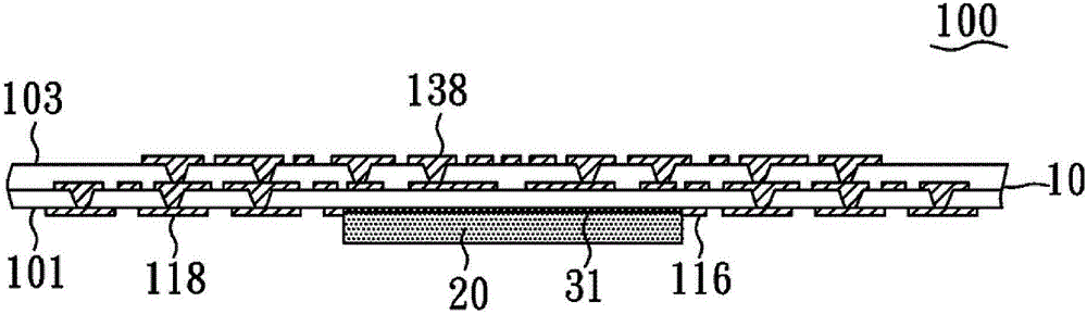
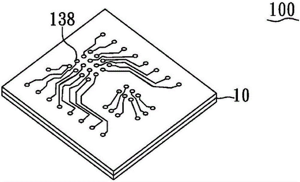
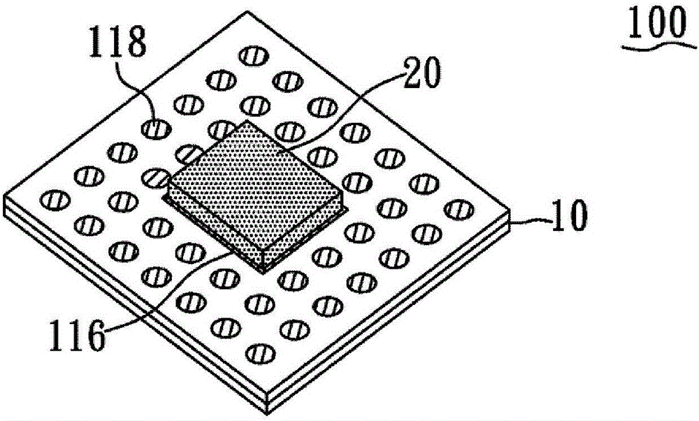
[0041] figure 1 , 2 and 3 are respectively a cross-sectional view, top and bottom perspective views of a low warpage coreless substrate 100 in an embodiment of the present invention, which includes a build-up circuit 10 and a bending resistance control member 20 .

[0042] Build-up circuit 10 has a bottom side 101 , an opposite top side 103 , contact pads 118 at bottom side 101 , and bond pads 138 at top side 103 . The contact pads 118 are formed outside the central area of ​​the bottom side 101 and are electrically coupled to the bonding pads 138 through vertical and lateral routing. In this figure, the pad pitch and pad size of the contact pads 118 are larger than the pad pitch and pad size of the bonding pads 138 , and the pad pitch and pad size of the bonding pads 138 are consistent with the I / O pads of the semiconductor device subsequently placed thereon. Thus, the semiconductor device with fine pads can be electrically coupled to the top side 103 of the build-up circui...

Embodiment 2

[0056] Figure 14 and 15 They are respectively a cross-sectional view and a top perspective view of another low warpage coreless substrate 200 in another embodiment of the present invention, which further includes a reinforcement layer.

[0057] In this embodiment, the low-warpage coreless substrate 200 is similar to that described in Embodiment 1, but the difference lies in that a reinforcement layer 40 is further provided on the top side 103 of the build-up circuit 10 . The reinforcement layer 40 has a through opening 405 extending through the reinforcement layer 40 between the top side and the bottom side, and is attached to the top side 103 of the build-up circuit 10 by the adhesive 33 . The reinforcement layer 40 covers the peripheral edge at the top side 103 of the build-up circuit 10, and the bonding pads 138 of the build-up circuit 10 are aligned with the through opening 405 of the reinforcement layer 40, and are exposed from above at the through opening 405 of the re...


PUM


Abstract

The invention discloses a coreless substrate including a build-up circuitry, a warping controller and an optional stiffener. The warping controller is adhered to the solder ball attachment side of the build-up circuitry and provides mechanical support for the coreless substrate, whereas the optional stiffener is positioned around peripheral edges of the coreless substrate at the chip attachment side of the build-up circuitry and provides mechanical support for the peripheral area of the coreless substrate.

Description

technical field [0001] The invention relates to a coreless substrate, in particular to a coreless substrate with a bending resistance control part and a semiconductor assembly thereof. Background technique [0002] The market trend of electronic devices (such as multimedia devices) tends to require faster and thinner designs. One of the methods is to interconnect semiconductor chips through a coreless substrate, so that the combined device can be thinner and signal integrity can be improved. US Patent Nos. 7,851,269, 7,902,660, 7,981,728 and 8,227,703 disclose various coreless substrates based on this purpose. However, since the coreless substrate is prone to warping due to repeated heating and cooling in the process, it is still not widely used. [0003] US Patent Nos. 9,185,799, 8,860,205, 7,981,728 and 7,902,660 attempt to address this problem with little success. In addition, the known methods of modifying the properties of the resin material or adding a reinforcement...

Claims


Application Information

Patent Timeline
Patent Type & Authority Applications(China)
IPC IPC(8): H01L23/498H05K1/02
CPCH01L23/49805H01L23/49822H01L23/49833H05K1/0271H05K2201/0133H01L2224/16227H01L2924/15311H01L2924/3511H01L23/49811H01L23/562
Inventor 林文强王家忠
Owner BRIDGE SEMICON
Why Eureka
Try Eureka