Array substrate and liquid crystal display panel

A technology for array substrates and display areas, applied in static indicators, nonlinear optics, optics, etc., can solve problems such as short circuits, and achieve the effect of improving display effects

Active Publication Date: 2016-09-21
WUHAN CHINA STAR OPTOELECTRONICS TECH CO LTD
View PDF6 Cites 7 Cited by
  • Summary
  • Abstract
  • Description
  • Claims
  • Application Information

AI Technical Summary

Problems solved by technology

[0003] The invention provides an array substrate and a liquid crystal display panel, which solves the problem of mutual short circuit caused by the positive and negative pola

Method used


Image

  • Array substrate and liquid crystal display panel
  • Array substrate and liquid crystal display panel
  • Array substrate and liquid crystal display panel

Examples


Embodiment Construction

[0018] The following will clearly and completely describe the technical solutions in the embodiments of the present invention with reference to the accompanying drawings in the embodiments of the present invention. Obviously, the described embodiments are only some, not all, embodiments of the present invention. Based on the embodiments of the present invention, all other embodiments obtained by persons of ordinary skill in the art without making creative efforts belong to the protection scope of the present invention.

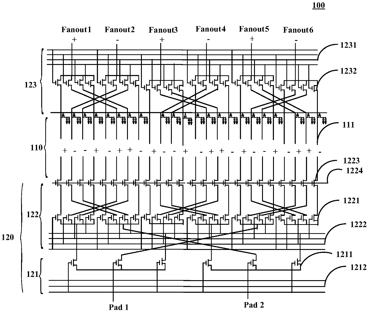
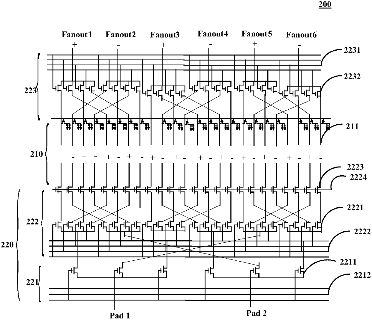
[0019] see figure 1 , figure 1 It is a structural schematic diagram of an array substrate provided by the present invention.

[0020] like figure 1 As shown, the array substrate 100 includes a display area 110 and a peripheral wiring area 120 .

[0021] Wherein, a plurality of data lines 111 are arranged in the display area 110 , and at least part of adjacent data lines 111 among the plurality of data lines 111 apply data driving signals with opposite polar...


PUM


Abstract

The invention discloses an array substrate and a liquid crystal display panel thereof. The array substrate comprises a display area and a peripheral wiring area, wherein a plurality of data lines are arranged in the display area, and at least one part of adjacent data lines of the plurality of data lines is applied with data driving signals withopposite polarities in the display process; a plurality of testing input ends and a testing distributing circuit are arranged in the peripheral wiring area; the testing distributing circuit is used for correspondingly connecting each testing input end to two data lines or more, so that each testing input end can apply testing signals to two data lines or more in the testing process; the testing distributing circuit is used for realizing the purpose that the data lines connected with each testing input end are applied with the data driving signals with same polarities in the display process. By adopting the type, the array substrate solves the problem of short-circuiting in the prior art because the positive and negative polarities of the two adjacent data lines are transferred to the same array testing point through a control switch in a polarity reversing mode.

Description

technical field [0001] The invention relates to the technical field of panel display, in particular to an array substrate and a liquid crystal display panel. Background technique [0002] In traditional small-size panel design, in order to improve the process yield of the array (Array) stage, an array test point (Array Test Pad) is designed at the end of the panel as the final barrier of yield control. After the cutting is completed, the array test pad and associated traces will remain on the panel. In order to avoid its influence on the normal display of the panel, a control switch is usually designed to realize the off state. However, due to the characteristics of the control switch itself, there will be a certain leakage current. Therefore, in the polarity inversion mode, it is easy to cause the positive and negative polarities between two adjacent data lines to be transmitted to the same array test point through the control switch, resulting in mutual short circuit, wh...

Claims


Application Information

Patent Timeline
IPC IPC(8): G02F1/133G02F1/1362G09G3/36
CPCG02F1/13306G02F1/136286G09G3/3614
Inventor 张婷婷王聪
Owner WUHAN CHINA STAR OPTOELECTRONICS TECH CO LTD
Why Eureka
Try Eureka