Supercharge Your Innovation With Domain-Expert AI Agents!

High-speed vertical channel three-dimensional NAND memory device

A memory and storage unit technology, applied in read-only memory, static memory, information storage, etc., can solve problems such as increased power consumption, increased number of string selection lines, and slow down component operations

Active Publication Date: 2019-06-18
MACRONIX INT CO LTD
View PDF2 Cites 0 Cited by
  • Summary
  • Abstract
  • Description
  • Claims
  • Application Information

AI Technical Summary

Problems solved by technology

Since the increase in memory layers also increases the number of string selection lines 12, it also results in increased power consumption and slows down device operations.

Method used


Image

  • High-speed vertical channel three-dimensional NAND memory device
  • High-speed vertical channel three-dimensional NAND memory device
  • High-speed vertical channel three-dimensional NAND memory device

Examples


Embodiment Construction

[0050] The following descriptions can provide any person of ordinary skill in the technical field with tools to use and make the present invention. The contents of this description are only provided for specific application and demand backgrounds. Modifications to the disclosed embodiments can be made by persons of ordinary skill in the art, and the general principles disclosed herein will be applicable to other embodiments and applications without departing from the spirit and scope of the invention. Therefore, the embodiments are presented only to illustrate the technical features of the present invention, not to limit the claims of the present invention.

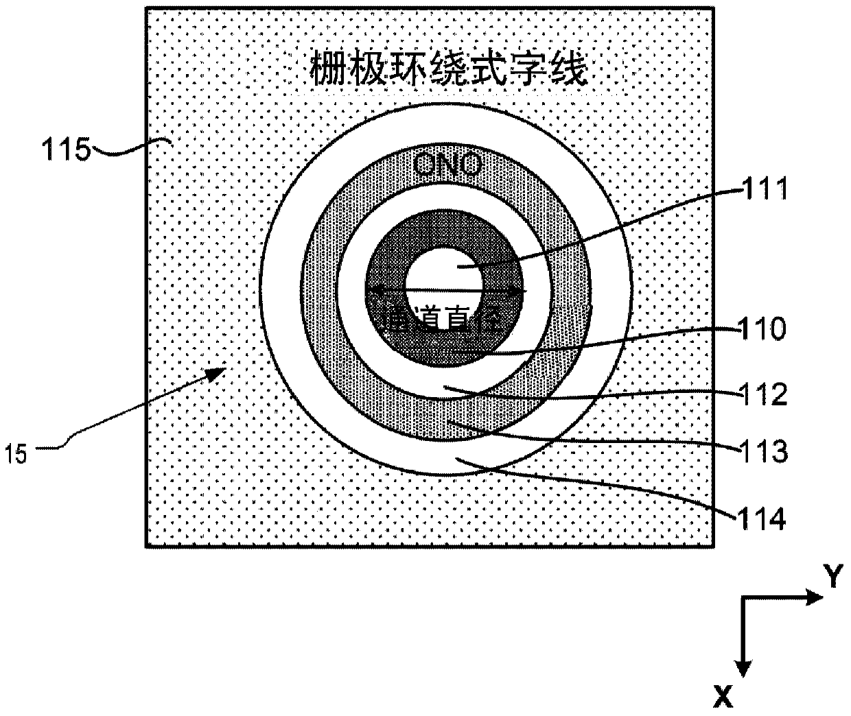
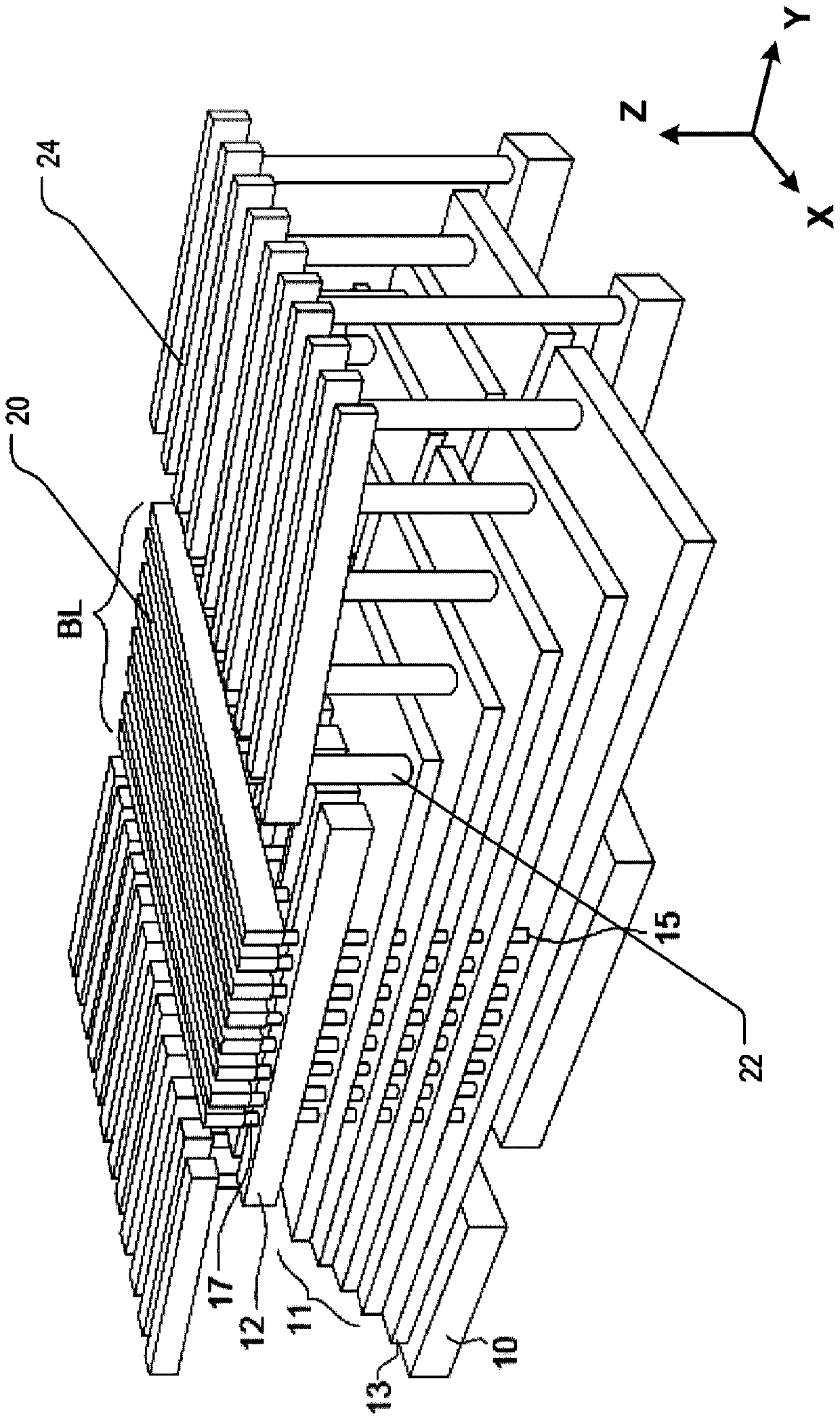
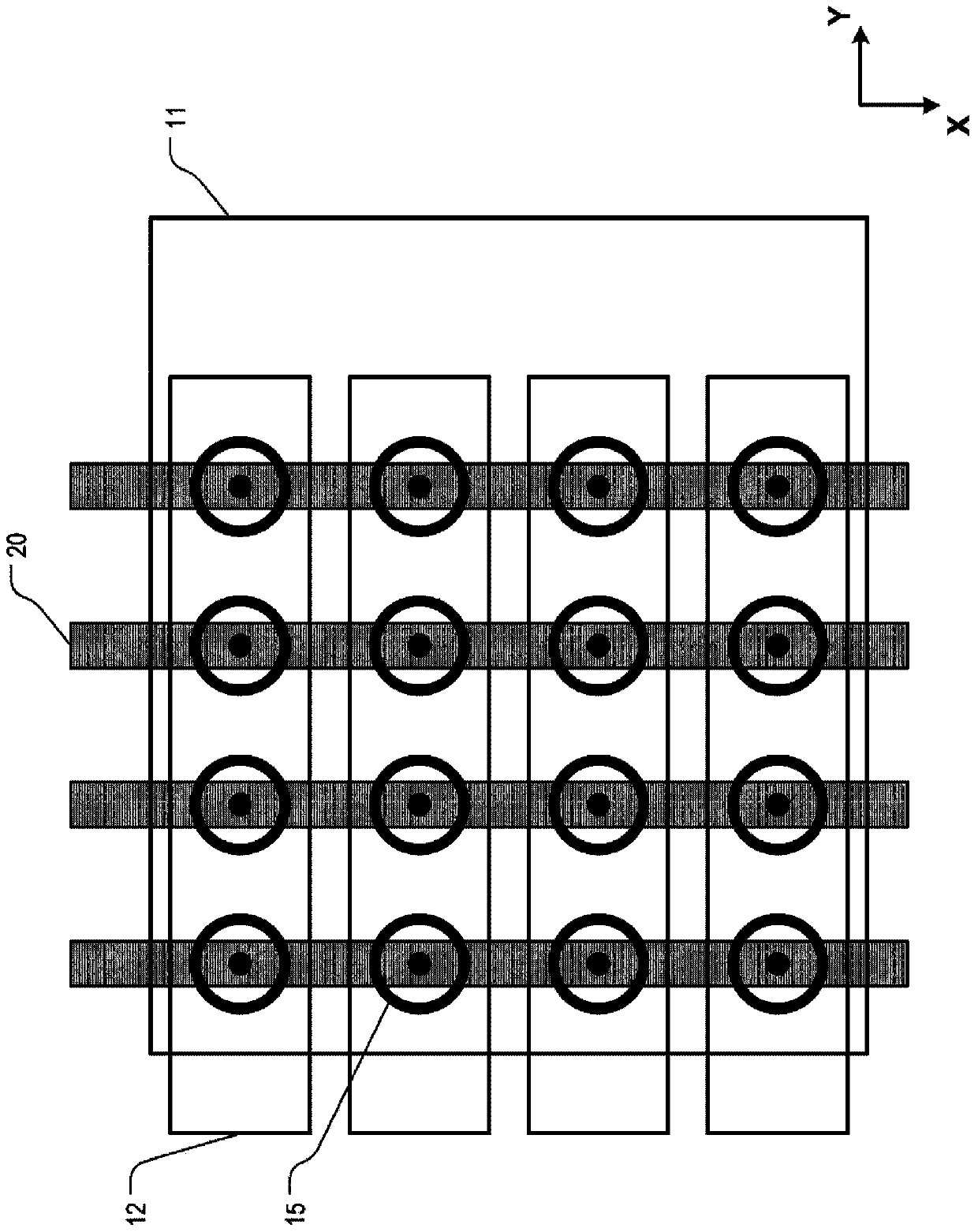
[0051] Figure 5 is instantiated at such as figure 2 with Figure 4 Top view of the columnar array in the depicted conventional 3D structure. Figure 5 Each dot (dot) in represents the lateral position of the corresponding columnar body 515 . As used herein, the "lateral" spatial dimension refers to the structural s...


PUM


Abstract

The invention provides a memory device. The memory device is provided with a plurality of stacked conductive layers. Each vertically-oriented cylindrical body comprises memory cells connected in series. The memory cells are arranged at the intersections between the cylindrical bodies and the conductive layers. String selection lines are arranged above the conductive layers, each intersection between the cylindrical bodies and the string selection lines defines a select gate of the cylindrical bodies. Bit lines pass above the String selection lines. The cylindrical bodies are arranged on a regular grid, wherein the regular grid is rotated relative to the bit lines. The grid may have square, rectangular or rhombic memory cells, and can be rotated by an angle [theta] relative to the bit lines by the equation tan([theta])=+ / -X / Y, wherein X and Y are co-prime integers. The string selection lines can be wide enough to intersect two cylindrical bodies at one side of the memory cells or all cylindrical bodies of the memory cells, or be wide enough to intersect two or more non-adjacent cylindrical bodies of the memory cells.

Description

technical field [0001] The present invention relates to a memory device having high density, and more particularly to a memory device configured with multi-planar memory cells to provide a three-dimensional (3D) array. Background technique [0002] As the critical dimensions of devices in integrated circuits shrink to the limits of typical memory cell technology, designers have sought techniques for stacking multi-planar memory cells to achieve greater storage capacitance and lower cost per bit. For example, Lai et al. published in "A Multi-Layer Stackable Thin-Film Transistor (TFT) NAND-Type Flash Memory," IEEE Int'l Electron Devices Meeting, 11-13 Dec. 2006, and Jung et al. in "Three Dimensionally Stacked NAND Flash Memory Technology UsingStacking Single Crystal Si Layers on ILD and TANOS Structure for Beyond 30nmNode,"IEEE Int'l Electron Devices Meeting, 11-13Dec.2006's technical content discloses that thin film transistor technology is applied to charge trapping memory t...

Claims


Application Information

Patent Timeline
Patent Type & Authority Patents(China)
IPC IPC(8): H01L27/1157H01L27/11582G11C16/06
Inventor 陈士弘
Owner MACRONIX INT CO LTD
Features
  • R&D
  • Intellectual Property
  • Life Sciences
  • Materials
  • Tech Scout
  • Unparalleled Data Quality
  • Higher Quality Content
  • 60% Fewer Hallucinations
Learn More