Check patentability & draft patents in minutes with Patsnap Eureka AI!

Inductive Load Voltage Pulse Width Modulation Degaussing Circuit

A pulse width modulation and degaussing circuit technology, applied in electrical components, pulse technology, electronic switches, etc., can solve the problems of large power consumption of Zener diodes or resistors, inability to quickly release inductive loads, breakdown of Zener diodes, etc. Achieve power saving, low power consumption and fast response

Active Publication Date: 2018-08-14
浙江桃园科技有限公司
View PDF8 Cites 0 Cited by
  • Summary
  • Abstract
  • Description
  • Claims
  • Application Information

AI Technical Summary

Problems solved by technology

Among them, the most widely used one is to control the MOS tube switch through the voltage pulse width modulation technology, and at the same time use the freewheeling diode to control the constant current of the inductive load, but every time the inductive load is cut off, due to the existence of the freewheeling diode and the current on the inductive load The reason for the inability to change abruptly is that the energy accumulated on the inductive load cannot be quickly released, resulting in a slow cut-off. The traditional solution is to connect a Zener diode and a freewheeling diode in series to realize freewheeling as a whole, or to A resistor and a freewheeling diode are connected in series to realize freewheeling as a whole. However, since the voltage pulse width modulation requires a high-speed switching MOS tube to control the current, it will cause the above-mentioned freewheeling to be frequently switched on and off, resulting in frequent switching of the Zener diode. The breakdown and the current flowing through the resistor are relatively large, which eventually leads to a large power consumption on the Zener diode or the resistor, so the traditional method cannot solve the above problems well, which requires a circuit to control the high-speed switching MOS tube in the voltage pulse width modulation When the inductive load is inductive, the Zener diode (or resistor) does not work, and when the inductive load is cut off, the Zener diode (or resistor) works, which can reduce the power consumption of the diode (or resistor)

Method used


Image

  • Inductive Load Voltage Pulse Width Modulation Degaussing Circuit
  • Inductive Load Voltage Pulse Width Modulation Degaussing Circuit
  • Inductive Load Voltage Pulse Width Modulation Degaussing Circuit

Examples


Embodiment Construction

[0033] The present invention will be further described below in conjunction with the accompanying drawings and embodiments.

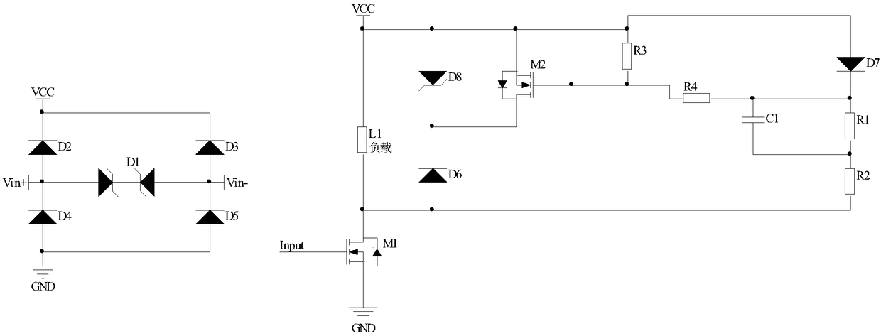
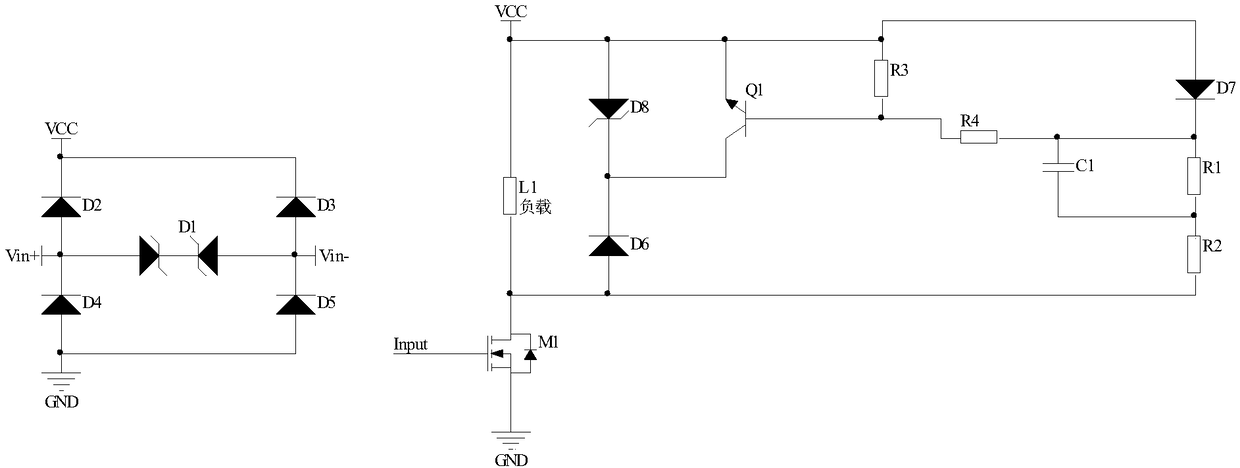
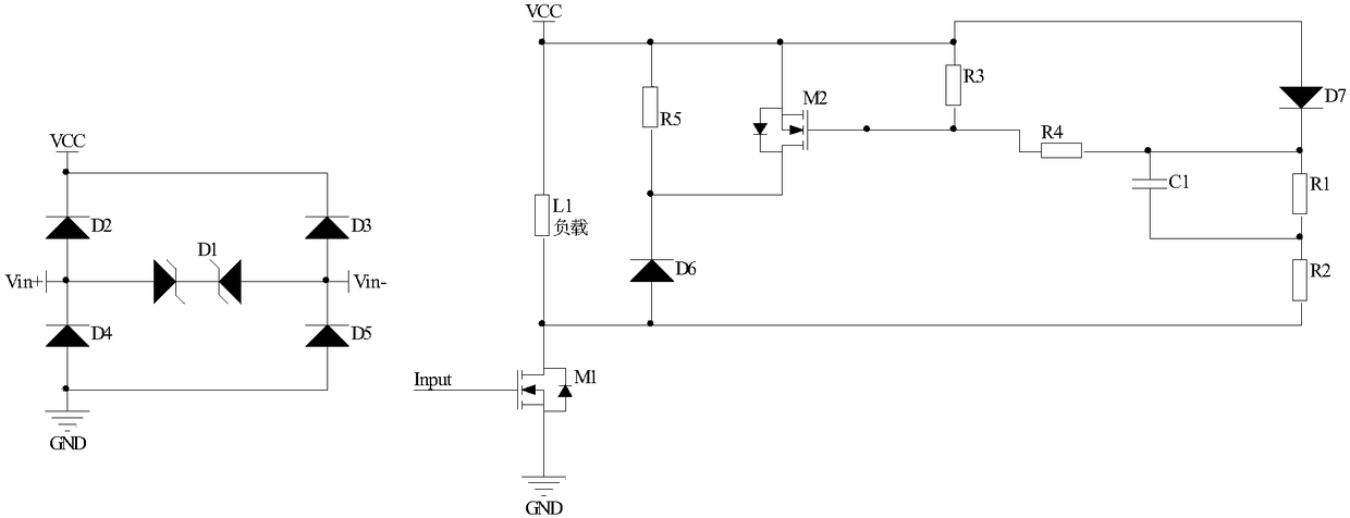
[0034] like figure 1 , figure 2 Shown, the present invention comprises input protection rectification circuit and demagnetization main circuit; Input protection rectification circuit comprises rectification diode D2, rectification diode D3, rectification diode D4, rectification diode D5 and bidirectional TVS tube or bidirectional voltage regulator diode D1; Demagnetization The main circuit includes NMOS tube M1, NMOS tube M2 or triode Q1, load L1, Zener diode D8, diode D6, diode D7, capacitor C1, resistor R1, resistor R2, resistor R3, resistor R4; one end of load L1 is connected to The anode of Zener diode D8, the source of NMOS transistor M2 or the emitter of transistor Q1, one end of resistor R3 and the anode of diode D7 are connected to VCC, and the other end of load L1 is respectively connected to the anode of diode D6 and the drain of NMOS transi...


PUM


Abstract

The invention discloses an inductive load voltage pulse width modulation demagnetizing circuit. The inductive load voltage pulse width modulation demagnetizing circuit comprises an input protection rectifying circuit and a main demagnetizing circuit. The input protection rectifying circuit is composed of a TVS tube or a bidirectional voltage-stabilizing diode and four rectifier diodes; the main demagnetizing circuit is composed of an NMOS tube M1, a load L1, a fly-wheel diode D6, a demagnetization voltage-stabilizing diode D8 (or a resistor), a bootstrap boost capacitor C1, a bootstrap boost auxiliary diode D7, a bootstrap boost capacitor charging and discharging loop control diode D10 (removable), a bootstrap voltage-dividing resistor R1 (removable), a bootstrap voltage-dividing resistor R2 (the resistance value can be zero), a driving voltage-dividing resistor R3, a driving voltage-dividing resistor R4 (the resistance value can be zero), a pulse width modulation stage conducting NMOS tube M2 (or triode), and an anti-NMOS tube breakdown voltage-stabilizing diode D9 (removable). The inductive load voltage pulse width modulation demagnetizing circuit is fast in response speed, simple in circuit, low in circuit cost, low in power consumption and fast in demagnetization.

Description

technical field [0001] The invention relates to a voltage pulse width modulation demagnetization circuit, in particular to an inductive load voltage pulse width modulation demagnetization circuit. Background technique [0002] With the rapid development of electronic technology, voltage pulse width modulation technology is more and more applied to various fields because it only needs to change the duty cycle to complete the linear control of the controlled object. Among them, the most widely used one is to control the MOS tube switch through the voltage pulse width modulation technology, and at the same time use the freewheeling diode to control the constant current of the inductive load, but every time the inductive load is cut off, due to the existence of the freewheeling diode and the current on the inductive load The reason for the inability to change abruptly is that the energy accumulated on the inductive load cannot be quickly released, resulting in a slow cut-off. Th...

Claims


Application Information

Patent Timeline
Patent Type & Authority Patents(China)
IPC IPC(8): H03K17/695
CPCH03K17/687
Inventor 姜文耀陶勇
Owner 浙江桃园科技有限公司
Features
  • R&D
  • Intellectual Property
  • Life Sciences
  • Materials
  • Tech Scout
  • Unparalleled Data Quality
  • Higher Quality Content
  • 60% Fewer Hallucinations
Learn More