
Wafer notch detection

一种晶片、缺口的技术,应用在位置的识别领域,能够解决展现增加复杂性及成本等问题

Active Publication Date: 2016-10-12
KLA CORP
View PDF3 Cites 0 Cited by
  • Summary
  • Abstract
  • Description
  • Claims
  • Application Information

AI Technical Summary

Problems solved by technology

All of which present increased complexity and cost

Method used


Image

  • Wafer notch detection
  • Wafer notch detection
  • Wafer notch detection

Examples


Embodiment Construction

[0014] Before stating the detailed description, it may be helpful to state definitions of certain terms that will be used hereinafter.

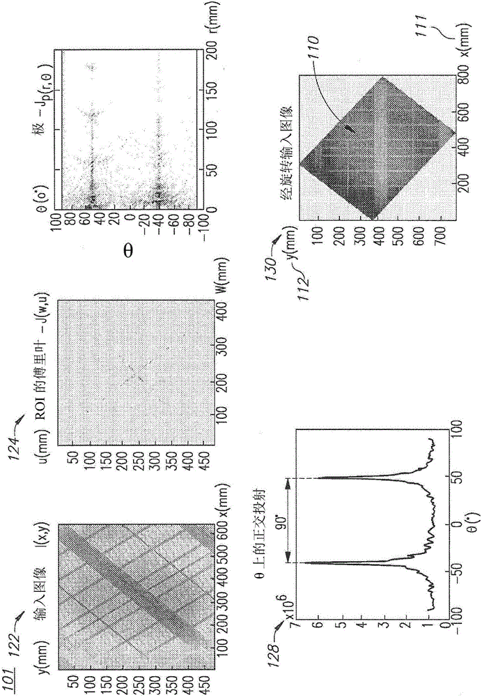
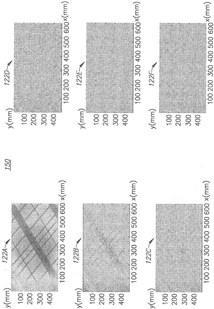
[0015] The term "geometric primitive" in an image as used in this application refers to basic forms, objects and patterns in an image, such as lines, simple shapes or recurring elements.

[0016] The term "deep track orientation" as used in this application refers to the orientation (eg, relative to a given grid) of a geometric primitive in an image. The term "track orientation algorithm" as used in this application refers to the way the track orientation is derived.

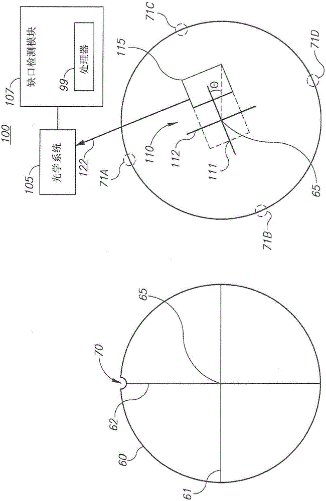
[0017] Note further that there is a strong geometric correlation between one wafer axis and the other wafer axis and between the main angle to one wafer axis and the main angle to the other wafer axis, respectively. Geometrically, the wafer axes are separated by multiples of 90°, as is the principal axis relative to the wafer axis. Thus, in the following description, any aspe...


PUM


Abstract

Notch detection methods and modules are provided for efficiently estimating a position of a wafer notch. Capturing an image of specified region(s) of the wafer, a principle angle is identified in a transformation, converted into polar coordinates, of the captured image. Then the wafer axes are recovered from the identified principle angle as the dominant orientations of geometric primitives in the captured region. The captured region may be selected to include the center of the wafer and / or certain patterns that enhance the identification and recovering of the axes. Multiple images and / or regions may be used to optimize image quality and detection efficiency.

Description

[0001] Related Application Cross Reference [0002] This application claims the benefit of US Provisional Patent Application Serial No. 61 / 939,131, filed February 12, 2014, which is hereby incorporated by reference in its entirety. technical field [0003] The present invention relates to the field of semiconductor technology, and more particularly, to the identification of the location of a wafer notch. Background technique [0004] Typically, the orientation of the wafer is conveyed by the location of the notch, which is indicative of the crystallographic orientation of the wafer. In the prior art, wafer orientation calculation based on notch orientation is time consuming since it requires an exhaustive search in the full angular range of 360 degrees. Typically, notch-only wafer orientation results are limited in accuracy and require an additional step of time-consuming "fine alignment". To avoid long mechanical movements, some of the existing solutions require addition...

Claims


Application Information

Patent Timeline
Patent Type & Authority Applications(China)
IPC IPC(8): H01L21/66
CPCH01L21/681G01B11/002G06T3/20G06T7/0004G06T7/60H01L22/12H01L22/26H01L2223/54493G06V10/42G01N21/8851G01N21/9501G06T2207/20056G06T2207/30148
Inventor B·埃弗拉蒂N·比沙拉A·西姆金Y·伊什-沙洛姆
Owner KLA CORP
Features
  • Generate Ideas
  • Intellectual Property
  • Life Sciences
  • Materials
  • Tech Scout
  • Unparalleled Data Quality
  • Higher Quality Content
  • 60% Fewer Hallucinations
Learn More