Broadband wave absorbing material with stable polarization

A wave-absorbing material and broadband technology, applied in the fields of wave-absorbing material, antenna communication and absorption shielding, can solve the problems of insufficient low-frequency bandwidth and poor polarization stability, so as to widen the working bandwidth, realize absorption and shielding, and enhance absorption and shielding. The effect of the wave effect

Active Publication Date: 2016-10-26
XIDIAN UNIV +1
View PDF6 Cites 36 Cited by
  • Summary
  • Abstract
  • Description
  • Claims
  • Application Information

AI Technical Summary

Problems solved by technology

[0006] The purpose of the present invention is to overcome the deficiencies in the above-mentioned prior art, and propose a polarization-stable broadband absorbing material, which is used to solve the problem of poor polarization stability and insufficient bandwidth in the low-frequency band existing in existing absorbing materials. technical problem

Method used


Image

  • Broadband wave absorbing material with stable polarization
  • Broadband wave absorbing material with stable polarization
  • Broadband wave absorbing material with stable polarization

Examples


Embodiment 1

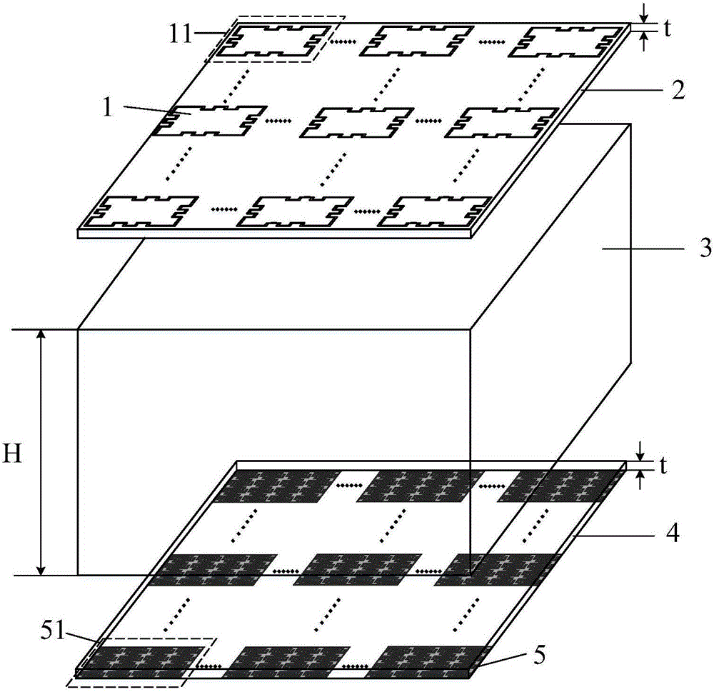
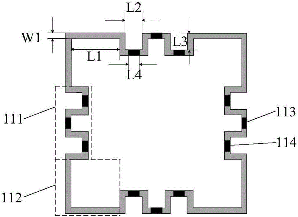
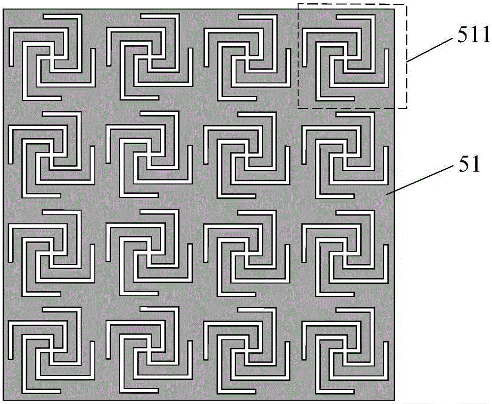
[0026] refer to figure 1 , the present invention includes a wave-absorbing structure 1, an upper dielectric plate 2, a foam layer 3, a lower dielectric plate 4 and a frequency selective surface 5; the wave-absorbing structure 1 is printed on the upper surface of the upper dielectric plate 2, and it The geometric center of the upper surface coincides; the frequency selective surface 5 is printed on the lower surface of the lower dielectric plate 4, and it coincides with the geometric center of the lower surface of the lower dielectric plate 4; the upper dielectric plate 2, the foam layer 3 and the lower dielectric plate 4 Arranged in order to form an up and down stacked structure, and the edges of the upper dielectric plate 2, the foam layer 3 and the lower dielectric plate 4 coincide with each other; the absorbing structure 1 is formed by periodic arrangement of M×N quasi-square metal folding line units 11, The frequency selective surface 5 is formed by periodic arrangement of...

Embodiment 2

[0030] The structure of embodiment 2 is identical with the structure of embodiment 1, and following parameter has been adjusted:

[0031] The arrangement periods of the metal fold line unit 11 and the frequency selective surface unit 51 are both 17 mm; the upper dielectric plate 2, the foam layer 3 and the lower dielectric plate 4 are all square plates with a side length of 170 mm, wherein the upper dielectric plate 2 and the lower dielectric plate The thickness of 4 is t=0.2mm, and the relative dielectric constant is 2.25; the metal line width W1=0.5mm of the metal folding line unit 11; the length of both arms of the equal-arm "L" type metal folding line 112 is L1=4.3mm; The width of the two grooves of the "bow"-shaped metal fold line 111 with a gap is L2=1.5mm, and the length of the gap is L4=1mm; the resistance value of the eight second chip resistors 114 is 40 ohms; the word "一" The edge distance S1 between the shaped groove 5112 and the folded line groove unit 511 is 0.22...

Embodiment 3

[0032] The structure of embodiment 3 is identical with the structure of embodiment 1, and following parameter has been adjusted:

[0033] The arrangement periods of the metal fold line unit 11 and the frequency selective surface unit 51 are both 16.2 mm; the upper dielectric plate 2, the foam layer 3 and the lower dielectric plate 4 are all square plates with a side length of 162 mm, wherein the upper dielectric plate 2 and the lower dielectric plate The thickness of plate 4 is t=0.2mm, and relative dielectric constant is 2.65; Foam layer 3 thickness H=15mm; The metal line width W1=0.5mm of metal folding line unit 11; The length of the arm is L1=4mm; the width of the two grooves of the "bow"-shaped metal fold line 111 with the gap is L2=1.5mm, and the length of the gap is L4=1mm; the resistance value of the eight second chip resistors 114 is 40 ohms; the distance S1 between the "one"-shaped slot 5112 and the edge of the folded line slot unit 511 is 0.125 mm.

[0034] Below in...


PUM


Abstract

The invention brings forward a broadband wave absorbing material with stable polarization, for solving the technical problems of poor polarization stability and not wide low-band bandwidth existing in a conventional wave absorbing material. The broadband wave absorbing material comprises a wave absorbing structure (1), an upper medium plate (2), a foam layer (3), a lower medium plate (4) and a frequency selection surface (5), wherein the wave absorbing structure (1) is printed on the upper surface of the upper medium plate (2), the frequency selection surface (5) is printed on the lower surface of the lower medium plate (4), the upper medium plate (2), the foam layer (3) and the lower medium plate (4) are successively arranged to form an up-down stacked structure, the wave absorbing structure (1) is formed by periodically arranging M*N metal broken line units (11) of dead square structures, and the frequency selection surface (5) is formed by periodically arranging M*N frequency selection surface units (51). The polarization stability is high, the absorption frequency band width is wide, the wave absorbing feature is high, the transmission feature at a high frequency is good, and the broadband wave absorbing material with stable polarization can be applied to such fields as antenna communication and absorption shielding and the like.

Description

technical field [0001] The invention belongs to the technical field of wave-absorbing materials, and relates to wave-absorbing materials and frequency-selective surfaces, in particular to a polarization-stable broadband wave-absorbing material, which has high polarization stability, wide absorption frequency band, and strong wave-absorbing properties , and has good transmission characteristics at high frequencies, and can be used in fields such as antenna communication and absorption shielding. Background technique [0002] With the rapid development of science and technology, there are more and more products that use electromagnetic waves to communicate with each other. The problem that follows is that electromagnetic waves have an increasing impact on the environment and human beings. For example, during the whole process of aircraft take-off, flight and landing, mobile communication equipment is required to be turned off throughout the entire process, in order to prevent ...

Claims


Application Information

Patent Timeline
Patent Type & Authority Applications(China)
IPC IPC(8): H01Q17/00
CPCH01Q17/00
Inventor 姜文薛晶晶张帅张胜辉董涛龚书喜
Owner XIDIAN UNIV
Why Eureka
Try Eureka