System, method, and computer device for adjusting antenna headroom of a pcb

A technology of antenna clearance area and adjustment module, which is applied in the direction of printed circuits connected with non-printed electrical components, electrical components, printed circuits, etc., can solve problems such as unfavorable antenna promotion and application, increased production costs, and decreased antenna radiation characteristics , to achieve the effect of promoting and applying and reducing production costs

Active Publication Date: 2018-09-11
GUANGDONG OPPO MOBILE TELECOMM CORP LTD
View PDF5 Cites 0 Cited by
  • Summary
  • Abstract
  • Description
  • Claims
  • Application Information

AI Technical Summary

Problems solved by technology

[0002] At present, in order to prevent the antenna from being easily interfered by other electronic components or metal devices on the printed circuit board PCB, resulting in a decrease in radiation characteristics, an antenna clearance area must be set on the printed circuit board PCB when the existing antenna is used in practice.
[0003] However, different antennas need to be configured with antenna clearance areas of different sizes. However, in the related art, once the antenna clearance area is set on the printed circuit board PCB, its area size will be fixed. At this time, in order to meet the needs of different antennas Application requirements, it is necessary to produce printed circuit board PCBs with antenna clearance areas of different areas, which not only increases the production cost, but also is not conducive to the promotion and application of antennas

Method used


Image

  • System, method, and computer device for adjusting antenna headroom of a pcb
  • System, method, and computer device for adjusting antenna headroom of a pcb
  • System, method, and computer device for adjusting antenna headroom of a pcb

Examples


Embodiment Construction

[0027] Embodiments of the present invention are described in detail below, examples of which are shown in the drawings, wherein the same or similar reference numerals designate the same or similar elements or elements having the same or similar functions throughout. The embodiments described below by referring to the figures are exemplary and are intended to explain the present invention and should not be construed as limiting the present invention.

[0028] The system, method and computer equipment for adjusting the antenna headroom of a printed circuit board PCB according to embodiments of the present invention will be described below with reference to the accompanying drawings.

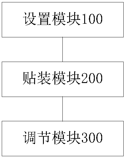
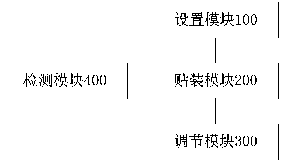
[0029] figure 1 is a schematic block diagram of a system for adjusting the antenna headroom of a printed circuit board PCB according to an embodiment of the present invention.

[0030] Such as figure 1 As shown, the system for adjusting the antenna headroom of a printed circuit board PCB includes...


PUM


Abstract

The invention discloses a system and method for adjusting an antenna clearance zone of a PCB, and computer equipment. The system is composed of a setting module, a mounting module, and an adjusting module. The setting module is used for setting an antenna clearance zone on a PCB body, wherein at least one antenna clearance zone is arranged. The mounting module is used for setting a welding plate at the bottom of the antenna clearance zone and at least one metal plate is mounted on the welding plate, wherein the at least one metal plate extend to the at least one antenna clearance zone externally. The adjusting module is used for adjusting the dimension of the metal plate, thereby adjusting the antenna clearance zone which the metal plate extends to externally. According to the system, an objective of adjustment of an area of an antenna clearance zone is achieved; and a phenomenon that a correlated enterprise needs to produce PCBs having antenna clearance zone with different areas to meet application requirements of different antennas can be avoided. Therefore, the production cost of the PCB is lowered and the antenna popularization and application can be realized well.

Description

technical field [0001] The invention relates to the technical field of printed circuit boards, in particular to a system for adjusting the antenna clearance area of ​​a printed circuit board PCB, a method for adjusting the antenna clearance area of ​​a printed circuit board PCB, and a computer device. Background technique [0002] At present, in order to prevent the antenna from being easily interfered by other electronic components or metal devices on the printed circuit board PCB, resulting in a decrease in radiation characteristics, an antenna clearance area must be provided on the printed circuit board PCB when the existing antenna is used in practice. [0003] However, different antennas need to be configured with antenna clearance areas of different sizes. However, in the related art, once the antenna clearance area is set on the printed circuit board PCB, its area size will be fixed. At this time, in order to meet the needs of different antennas According to applicati...

Claims


Application Information

Patent Timeline
Patent Type & Authority Patents(China)
IPC IPC(8): H05K1/18
CPCH05K1/183H05K2201/10568
Inventor 罗群
Owner GUANGDONG OPPO MOBILE TELECOMM CORP LTD
Why Eureka
Try Eureka