Touch module and touch input system

A touch module and input system technology, applied in the field of touch input systems and touch modules, can solve the problems of poor precision, limited wiring area of ​​capacitive touch screen, unsuitable for long-term development, etc., and achieve the goal of reducing production costs Effect

Pending Publication Date: 2017-01-04
HEFEI BOE OPTOELECTRONICS TECH +1
View PDF9 Cites 5 Cited by
  • Summary
  • Abstract
  • Description
  • Claims
  • Application Information

AI Technical Summary

Problems solved by technology

[0004] The active capacitive pen is a stylus solution implemented on the basis of the hardware of the existing capacitive touch screen system, so it is necessary to consider the light transmittance, which causes the wiring area of ​​the capacitive touch screen to be severely limited, thereby limiting the size of the touch sensor. It directly affects the accuracy of the capacitive touch screen, which fundamentally deviates from the narrow frame required by users; and the larger the product size, the worse the accuracy and the higher the cost, which is not suitable for long-term development
[0005] In addition, the currently widely used active capacitive pens are not perfectly compatible with finger touch on most products, that is to say, when using a pen, you can no longer use your fingers to touch at the same time, which limits the user experience. , and the current popular active capacitive pens are difficult to achieve real multi-touch with multiple active pens

Method used


Image

  • Touch module and touch input system
  • Touch module and touch input system
  • Touch module and touch input system

Examples


Embodiment Construction

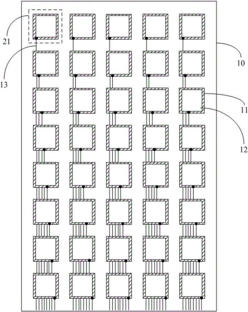
[0028] Embodiments of the present invention provide a touch module and a touch input system, which are used to realize the transmittance without affecting the display module and reduce the cost of material selection.

[0029] In order to make the purpose, technical solutions and advantages of the present invention clearer, the present invention will be further described in detail below in conjunction with the accompanying drawings. Obviously, the described embodiments are only some of the embodiments of the present invention, rather than all of them. Based on the embodiments of the present invention, all other embodiments obtained by persons of ordinary skill in the art without making creative efforts belong to the protection scope of the present invention.

[0030] The touch module provided by specific embodiments of the present invention will be described in detail below in conjunction with the accompanying drawings.

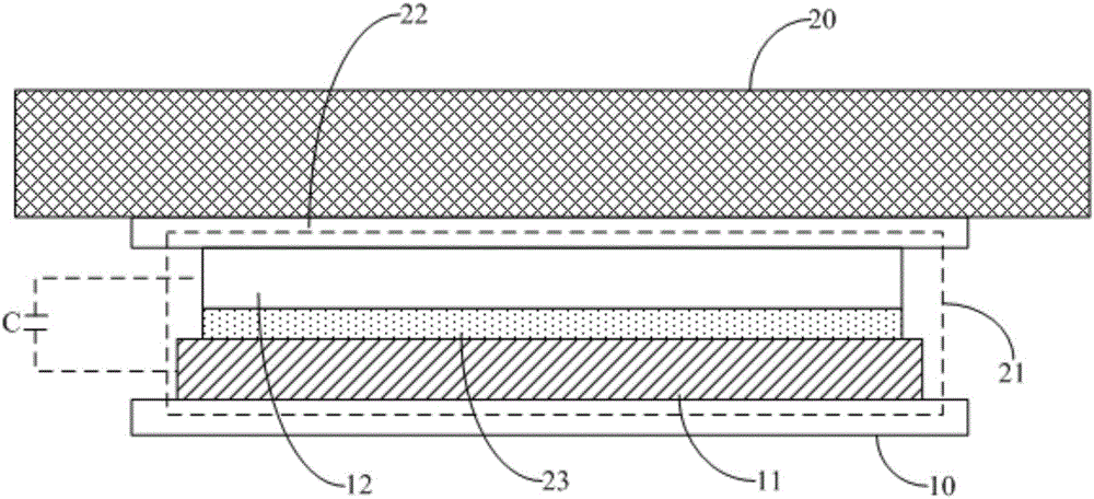
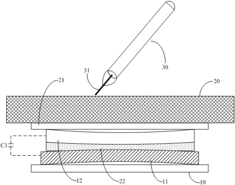
[0031] The thickness, area size, and shape of each film ...


PUM


Abstract

The invention discloses a touch module and a touch input system. The touch module and the touch input system are used for reducing material cost without influencing the permeability of a display module. The touch module comprises the display module, a magnetic sensor module and a touch detecting circuit. The magnetic sensor module is arranged below the display module, and comprises a base, a plurality of magnetic sensor units arranged on the base in arrays and a plurality of wires. Each magnetic sensor unit comprises a first substrate and a second substrate which are oppositely arranged, and an insulating medium which is located between the first substrate and the second substrate. The magnetic polarity of the first substrate and the magnetic polarity of the second substrate are opposite. Capacitance is formed between the first substrate and the second substrate. Each magnetic sensor unit is connected with one wire which is used for making the magnetic sensor unit connected with the touch detecting circuit. The touch detecting circuit is used for determining the touched position of the display module by detecting the magnitude of the capacitance between the first substrate and the second substrate.

Description

technical field [0001] The present invention relates to the field of display and touch technology, in particular to a touch module and a touch input system. Background technique [0002] With the rapid development of smart phones and tablet computers, touch screens have been widely used in daily life. At present, the most popular is the capacitive touch screen. When the finger is in contact with the screen, the touch screen will calculate the position of the finger through the current generated by the capacitance change. The accuracy of the capacitive touch screen can reach several pixels in theory, but the actual effective range is in It is about 1 square centimeter, so fingers are generally used for operation on current mainstream capacitive touch screen mobile phones. [0003] However, whether it is writing or drawing on the screen of the mobile phone, the lines of the handwriting are very thick, and the accuracy of the strokes is poorly controlled. However, more and mor...

Claims


Application Information

Patent Timeline
Patent Type & Authority Applications(China)
IPC IPC(8): G06F3/041G06F3/044G06F3/046G06F3/0354
CPCG06F3/03545G06F3/0412G06F3/0416G06F3/044G06F3/046G06F2203/04108
Inventor 呼艳生方志祥潘卫卫杨光磊张忠琪
Owner HEFEI BOE OPTOELECTRONICS TECH
Why Eureka
Try Eureka