Imaging element including a photoelectric conversion unit and a charge transfer path for transferring generated charges
A photoelectric conversion part and charge transmission technology, which is applied in the direction of electrical components, TV system components, circuits, etc., can solve problems such as the influence of high-speed movement of shooting components, and achieve the effect of high time resolution
- Summary
- Abstract
- Description
- Claims
- Application Information
AI Technical Summary
Problems solved by technology
Method used
Image

Examples
no. 1 approach
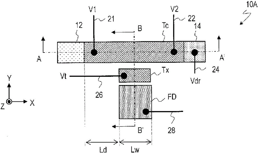
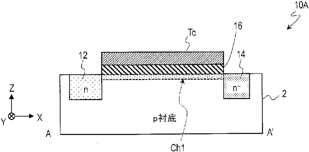
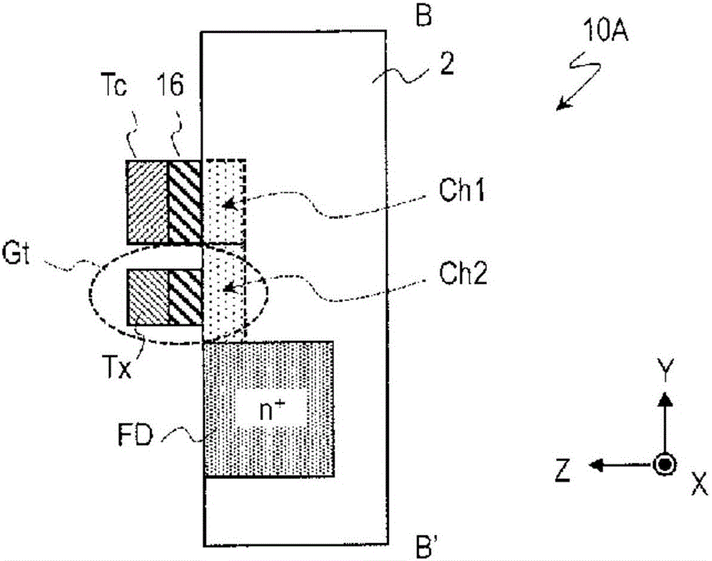
[0122] Figure 1 ~ Figure 3 An example of the pixel structure in the imaging element according to the first embodiment of the present application is schematically shown. figure 1 The arrangement of each part constituting the pixel when viewed from the normal direction of the imaging surface is schematically shown. figure 2 and image 3 represent schematically figure 1 The A-A' line section and the BB' line section are shown. Figure 1 ~ Figure 3 In FIG. 2 , for reference, arrows indicating X directions, Y directions, and Z directions perpendicular to each other are shown in the drawings. The Z direction is the normal direction of the imaging surface. In other drawings, arrows indicating the X direction, the Y direction, or the Z direction may also be illustrated.
[0123] Figure 1 ~ Figure 3 The illustrated pixel 10A includes a photoelectric conversion portion 12 , a drain 14 , and a charge accumulation portion FD. in addition, Figure 1 ~ Figure 3 These are merely s...
no. 2 approach
[0166] Figure 8 An example of the pixel structure in the imaging element of the second embodiment of the present application is schematically shown. Figure 8 shown in the Pixel 10C with figure 1 The illustrated pixel 10A is different in that the pixel 10C has a plurality of charge accumulation portions arranged along the charge transfer path Ch1.
[0167] exist Figure 8 In the illustrated structure, four charge accumulation portions FDa to FDd having a length Lw in the X direction are arranged along the X direction with a gap g. Figure 8 The number of charge storage portions shown, the length (width) in the direction along the charge transfer path Ch1 , and the interval between two adjacent charge storage portions are merely examples. For example, the number of charge storage portions included in each pixel is not limited to four, and the width or interval may be different among a plurality of charge storage portions.
[0168] exist Figure 8 In the illustrated config...
no. 3 approach
[0197] Figure 16 An example of the pixel structure in the imaging element according to the third embodiment of the present application is schematically shown. Figure 16 shown in the Pixel 10F with Figure 8 The pixel 10C shown differs in that the pixel 10F has multiple transfer gate electrodes.
[0198] exist Figure 16 In the illustrated configuration, transfer gate electrodes Txa to Txd are arranged between the charge transfer path Ch1 and the charge storage parts FDa to FDd so as to correspond to the charge storage parts FDa to FDd, respectively. As shown in the figure, the transfer gate electrodes Txa to Txd are respectively connected to the gate control lines 26a to 26d, and therefore, the respective transfer gate electrodes Txa to Txd are configured to independently apply the gate control voltages Vta to Vtd. That is, the pixel 10F has the same number (here, four) of gate electrodes as the charge accumulation portions arranged along the charge transfer path Ch1 . T...
PUM
 Abstract
Description
Claims
Application Information
PatSnap Eureka turns technology decisions into work you can execute. Powered by our Innovation Knowledge Graph, it runs expert workflows across engineering, life sciences, materials and intellectual property. Get your review-ready output in minutes.


