Gate linewidth tailoring and critical dimension control for sub-100 nm devices using plasma etching

a technology of plasma etching and line width, which is applied in the direction of photosensitive material processing, photomechanical equipment, instruments, etc., can solve the problem that the process of simply developing a lithographic image projected onto the wafer no longer provides the critical dimension required

Inactive Publication Date: 2005-03-08
INT BUSINESS MASCH CORP
View PDF15 Cites 403 Cited by
  • Summary
  • Abstract
  • Description
  • Claims
  • Application Information

AI Technical Summary

Benefits of technology

An object of the present invention to provide a method for achieving sub-resolution features on an electronic chip than possible using a single mask process and conventional lithography by allowing patterning of sub-lithographic (as printed) dimensions on a wafer.
In view of the foregoing and other problems, this invention solves this problem by providing a method to achieve very tight tolerance on variation of lines by printing a first mask on a wafer, referred to as a soft mask, using conventional photolithographical techniques well known in the art. This soft mask is then trimmed using a precisely-defined set of etch conditions. This trimmed soft mask is then used to define (etch) the hard-mask, which is subsequently used to etch one or more layers on the wafer itself Conditions of this second etch are likewise very precisely-defined. The desired effect achieved in this dual masking technique is a minimum linewidth variation in isolated feature versus nested features.

Problems solved by technology

As features on electronic chips have become smaller, a point is eventually reached in which the conventional process of simply developing a lithographic image projected onto the wafer no longer provides the required Critical Dimension (CD).

Method used


Image

  • Gate linewidth tailoring and critical dimension control for sub-100 nm devices using plasma etching
  • Gate linewidth tailoring and critical dimension control for sub-100 nm devices using plasma etching

Examples


Embodiment Construction

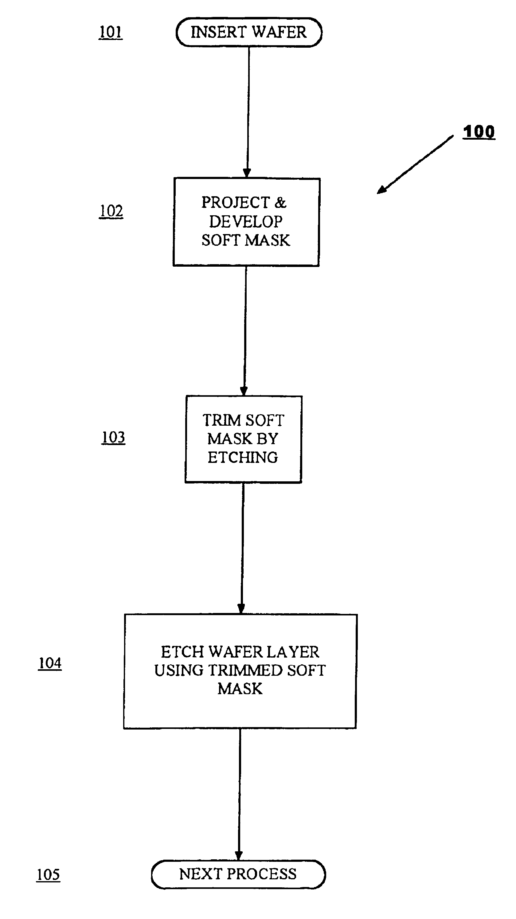
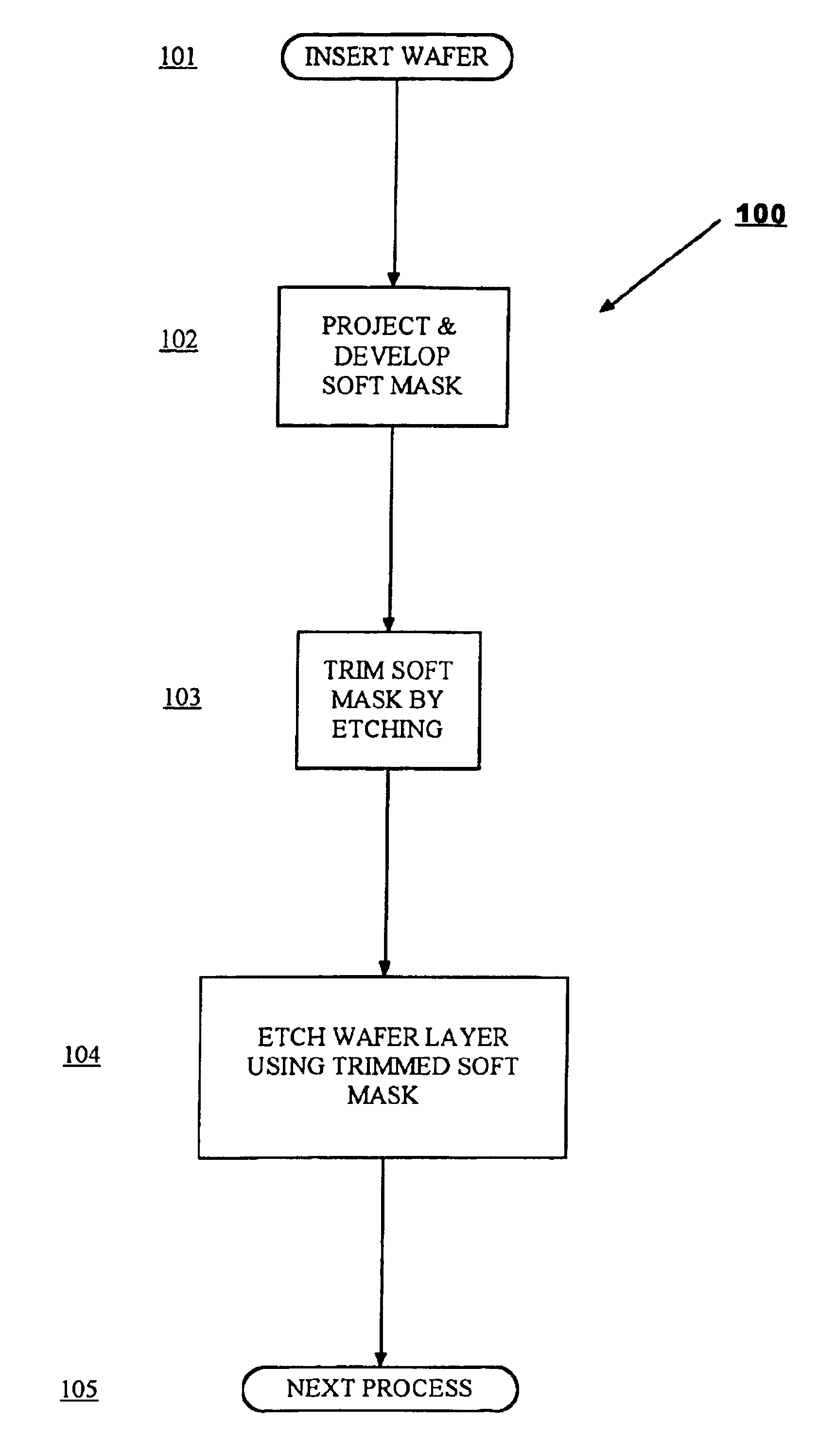
Referring now to the drawing, a basic technique is discussed in which a first mask, referred to as a soft mask, is developed on a wafer and then trimmed using a precisely tuned etching process to etch the developed masking material. The resultant trimmed mask is then used as a mask to etch a layer on the wafer, again using a precisely tuned etching process different from the previous etch by reason of having now to etch a material on the wafer rather than the mask material.

Not only is the dual etching process novel but the disclosure additionally provides a range of conditions that optimize each of the two etching steps. The inventors have developed and investigated this technique in a standard capacitively coupled plasma reactor. However, the basic technique can easily be expanded into other etching techniques, conditions, and combinations than the precise conditions described herein.

Referring now to the FIGURE, a wafer is introduced (step 101) into the environment appropriate to p...


PUM

PropertyMeasurementUnit
widthaaaaaaaaaa
RF poweraaaaaaaaaa
pressureaaaaaaaaaa

Abstract

A method of fabricating an electronic chip on a wafer in which a first mask at a predetermined lower resolution is developed on the wafer and then etched under a first set of conditions for a predetermined period to achieve a mask that is below the resolution limit of current lithography. The etched mask is then used as a hard mask for etching material on a lower layer.

Description

BACKGROUND OF THE INVENTION1. Field of the InventionThe present invention generally relates to maintaining variation tolerances of line widths for electronic chip fabrication in sub-100 nm devices. Specifically, a precisely-tuned trimming plasma etch procedure for a first soft mask is followed by a precisely defined oxide hard-mask etch procedure to result in a process that achieves minimum linewidth variation tolerances from the nominal value, not only for the vertical versus horizontal dimension but also for variations between isolated features versus nested features.2. Description of the Related ArtAs features on electronic chips have become smaller, a point is eventually reached in which the conventional process of simply developing a lithographic image projected onto the wafer no longer provides the required Critical Dimension (CD). Critical dimension (or gate line-width) control has become increasingly important for Sub-100 nm devices. At these small feature sizes, not only is...

Claims


Application Information

Patent Timeline
Patent Type & Authority Patents(United States)
IPC IPC(8): G03F7/40G03F7/42H01L21/033
CPCG03F7/40H01L21/0338H01L21/0337G03F7/427
Inventor BROWN, JEFFREY J.DESHPANDE, SADANAND VINAYAKHORAK, DAVID V.SURENDRA, MAHESWARANTSOU, LEN Y.YANG, QINGYUNYU, CHIENFANZHANG, YING
Owner INT BUSINESS MASCH CORP
Why Eureka
Try Eureka