Method and device for reducing fixed pattern noise of image sensor in digital domain

An image sensor and pattern technology, applied in the field of image sensor fixed pattern noise reduction and noise elimination mechanism, can solve the problems of inconsistent circuit signal characteristics, circuit interference, complicated circuit design, etc., and achieve the effect of avoiding signal processing time

Active Publication Date: 2019-07-26
PIXART IMAGING INC
View PDF5 Cites 0 Cited by
  • Summary
  • Abstract
  • Description
  • Claims
  • Application Information

AI Technical Summary

Problems solved by technology

[0002] Generally speaking, a traditional image sensor has the non-ideal effect of the analog circuit, resulting in the presence of noise on the image sensing screen.
For example, noise from non-ideal effects of analog circuits may include fixed pattern noise on the screen, that is, the phenomenon of straight lines on the sensing screen, which is caused by traditional sensor arrays. Leakage current, resulting in inconsistent signal characteristics of each straight-line circuit, resulting in a straight line phenomenon on the final sensing screen. In addition, the stray capacitance in the traditional image sensor is also easy to cause each straight-line circuit to be affected when the analog signal is switched. Interference causes the signal characteristics of each direct circuit to be inconsistent, and this is also one of the causes of fixed pattern noise
Furthermore, the analog circuit of the traditional image sensor also has other noises (such as random noise), which will also affect the image sensing screen
In order to reduce the noise caused by the non-ideal effect of the analog circuit in the current existing technology, the noise elimination circuit is usually implemented in the analog domain to reduce the noise. However, such a circuit design will be too complicated, and the circuit cost is also high

Method used


Image

  • Method and device for reducing fixed pattern noise of image sensor in digital domain
  • Method and device for reducing fixed pattern noise of image sensor in digital domain

Examples


Embodiment Construction

[0015] It should be understood that the specific embodiments described here are only used to explain the present invention, not to limit the present invention.

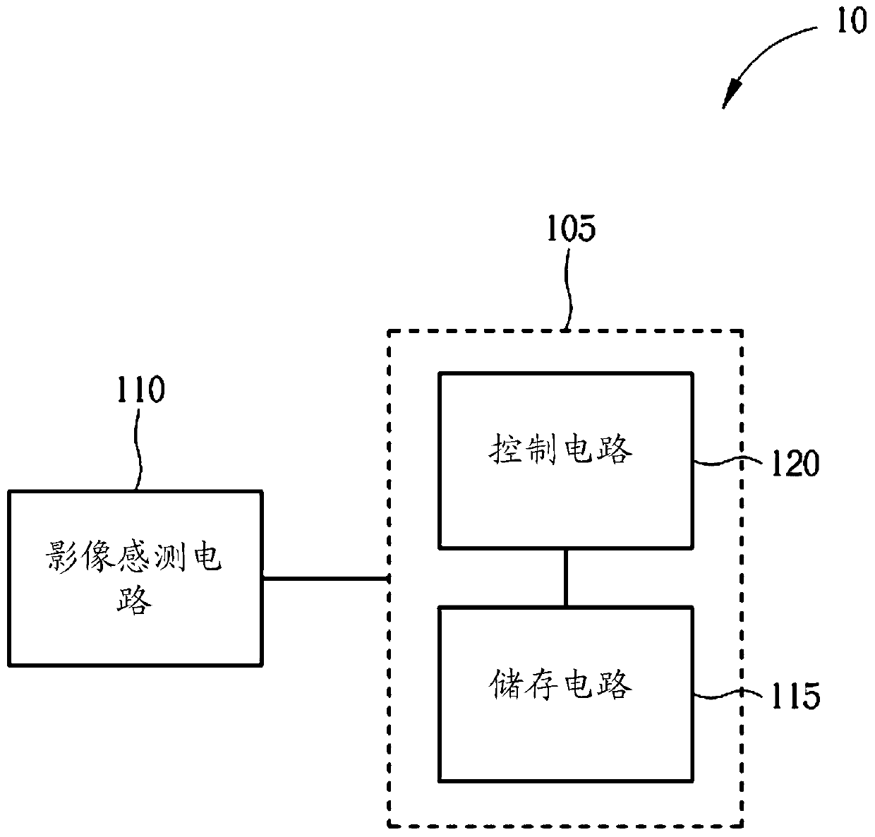
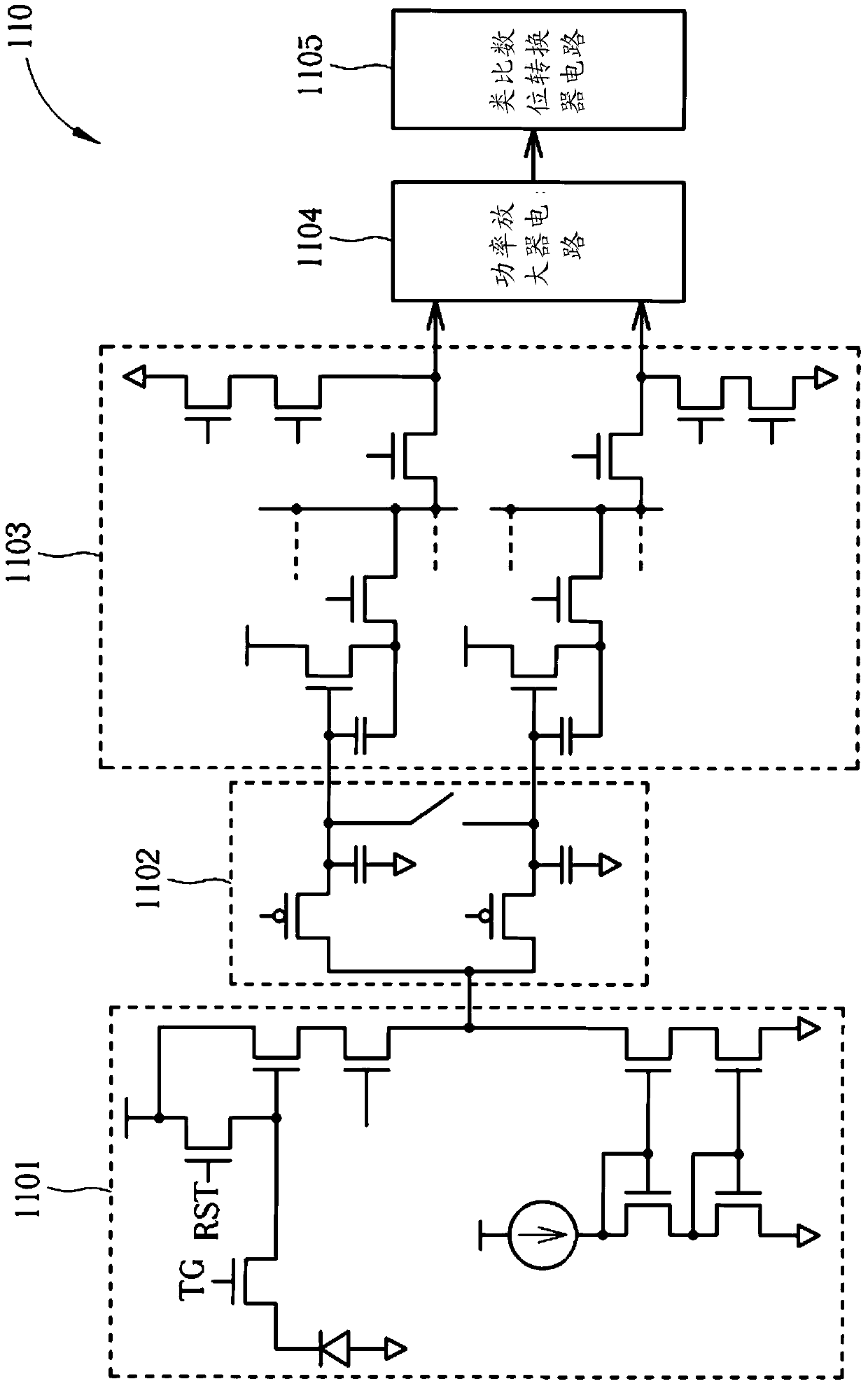
[0016] Please refer to figure 1 and figure 2 , figure 1 It is a schematic diagram of a device 105 used in an image sensor 100 to adjust the noise caused by the non-ideal effect of an analog circuit according to an embodiment of the present invention. The image sensor 100 includes an image sensing circuit 110 and used to adjust the noise of pixel data means 105, figure 2 Yes figure 1 A schematic diagram of an exemplary circuit of the image sensing circuit 110 is shown. The device 105 can be regarded as a calibration device / circuit and includes a storage circuit 115 and a control circuit 120. In addition, the image sensing circuit 110 includes a sensing pixel array 1101, a second sampling circuit (Correlated Double Sampling (CDS) Circuit ) 1102, a source follower circuit 1103, a power amplifier circuit 1104, and ...


PUM


Abstract

The invention provides a method of reducing fixed pattern noise of an image sensor in a digital domain. The method comprises steps: in a test environment, pixel data for at least one test picture are accessed; the average value of at least one part of pixel data for the at least one test picture in each row is calculated; and the average value in each row is used as a correction value for image data in each row in a normal light source environment to reduce the fixed pattern noise of the image sensor. The invention also provides a device for reducing the fixed pattern noise of the image sensor in the digital domain. By adopting the method and the device of the invention, the fixed pattern noise of the image sensor can be reduced.

Description

technical field [0001] The invention relates to a noise elimination mechanism in the field of image sensing, in particular to a method and device for reducing fixed pattern noise of an image sensor. Background technique [0002] Generally speaking, a traditional image sensor has the non-ideal effect of the analog circuit, which causes noise on the image sensing screen. For example, noise from non-ideal effects of analog circuits may include fixed pattern noise on the screen, that is, the phenomenon of straight lines on the sensing screen, which is caused by traditional sensor arrays. Leakage currents lead to inconsistencies in the signal characteristics of each straight-line circuit, causing straight lines to appear on the final sensing screen. In addition, the stray capacitance in traditional image sensors also easily causes each straight-line circuit to be affected when the analog signal is switched. Interference causes the signal characteristics of each direct circuit to...

Claims


Application Information

Patent Timeline
Patent Type & Authority Patents(China)
IPC IPC(8): H04N5/357H04N5/365
Inventor 周健荣叶梅昭颜文正
Owner PIXART IMAGING INC
Why Eureka
Try Eureka