Circuit probing system and its circuit probing device
A technology of circuit detection and probe, which is applied in the direction of measuring device, electronic circuit test, measuring device shell, etc., can solve the problem of damaging the probe card probe, affecting the electrical performance and test results of the probe card, and accidentally touching the probe card probe. Needle and other issues
- Summary
- Abstract
- Description
- Claims
- Application Information
AI Technical Summary
Problems solved by technology
Method used
Image

Examples
no. 1 approach
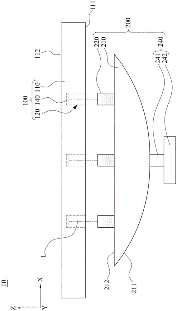
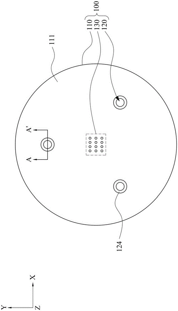
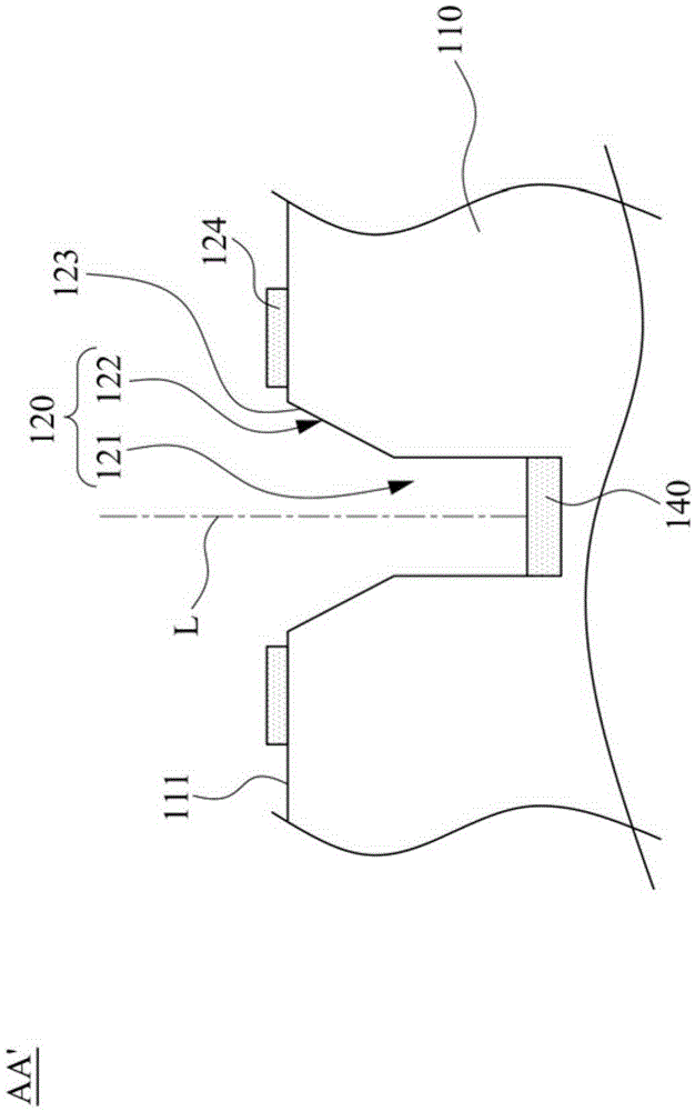
[0033] figure 1 An exploded view of the probe card 100 and the protective cover 200 of the circuit detection device 10 according to the first embodiment of the present invention is shown. figure 2 draw figure 1 The top view of the probe card 100. Such as figure 1 and figure 2 As shown, the circuit detection device 10 includes a probe card 100 and a protective cover 200 . The probe card 100 includes a substrate body 110 , a probe area 130 and a plurality of first magnetic attractors 140 . The substrate body 110 has a front side 111 and a back side 112 opposite to each other. The probe area 130 is disposed on the front surface 111 of the substrate body 110 . A plurality of openings 120 are also formed on the front surface 111 of the substrate body 110 . Each first magnetic element 140 is fixed in one of the openings 120 and connected to the substrate body 110 . The protective cover 200 is removably fixed on the probe card 100 . The protection cover 200 includes a cove...
no. 2 approach
[0044] The circuit detection device of the second embodiment is substantially the same as the circuit detection device of the first embodiment, except that the second magnetic attraction part 220 of the first embodiment is composed of permanent magnets as a whole ( figure 1 ), on the other hand, Figure 4 A schematic diagram of the second magnetic member 230 of the protective cover 201 according to the second embodiment of the present invention is shown. Such as Figure 4 As shown, the second magnetic element 230 includes a columnar body 231 and a magnetic block 232 . The columnar body 231 is located between the magnetic block 232 and the cover 210 so as to attract each other with the first magnetic member.
[0045] so, compared to figure 1 The second magnetic piece 220 is a permanent magnet as a whole. In the second embodiment, a smaller magnetic block 232 is arranged at the end of the columnar body 231 to attract each other with the first magnetic piece. Not only can it b...
no. 3 approach
[0047] Figure 5A to Figure 5B A schematic diagram of the operation of the circuit detection system 1 according to the third embodiment of the present invention is shown. Such as Figure 5A to Figure 5B As shown, in this embodiment, the circuit detection system 1 includes the above-mentioned circuit detection device 10 , a pick-up device 300 and a transmission device 400 . The circuit detection device 10 of the third embodiment adopts all the features of the circuit detection devices of the above-mentioned embodiments. The pick-up device 300 is used to disengage the protective cover 200 from the probe card 100 in a straight line in a second direction (such as Z-axis downward) by moving the holding portion 240 . The transmission device 400 is electrically connected to the fetching device 300 to drive the fetching device 300 to move. The transmission device 400 is, for example, a known technology such as a motor or a cylinder. However, the present invention is not limited the...
PUM
 Abstract
Description
Claims
Application Information
 - R&D
- Intellectual Property
- Life Sciences
- Materials
- Tech Scout
- Unparalleled Data Quality
- Higher Quality Content
- 60% Fewer Hallucinations
Browse by: Latest US Patents, China's latest patents, Technical Efficacy Thesaurus, Application Domain, Technology Topic, Popular Technical Reports.
© 2025 PatSnap. All rights reserved.Legal|Privacy policy|Modern Slavery Act Transparency Statement|Sitemap|About US| Contact US: help@patsnap.com