Supercharge Your Innovation With Domain-Expert AI Agents!

Inductance structure, flexible circuit board and fabrication method

A technology of flexible circuit boards and manufacturing methods, which is applied in the direction of multi-layer circuit manufacturing, printed circuits connected with non-printed electrical components, printed circuits, etc., and can solve problems such as unfavorable development of thin electronic products and large thickness of circuit boards

Inactive Publication Date: 2017-03-01
AVARY HLDG (SHENZHEN) CO LTD +2
View PDF6 Cites 1 Cited by
  • Summary
  • Abstract
  • Description
  • Claims
  • Application Information

AI Technical Summary

Problems solved by technology

The thickness of the circuit board with embedded inductance structure produced by this method is relatively large, which is not conducive to the development of thinner modern electronic products

Method used


Image

  • Inductance structure, flexible circuit board and fabrication method
  • Inductance structure, flexible circuit board and fabrication method
  • Inductance structure, flexible circuit board and fabrication method

Examples


Embodiment Construction

[0042] Combine below Figure 1~Figure 27 And the embodiments further illustrate the flexible circuit board and the manufacturing method of the flexible circuit board provided by the present invention.

[0043] see Figure 1~Figure 13 , the manufacturing method of the flexible circuit board 100 provided by the first embodiment of the present invention is as follows:

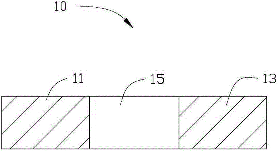
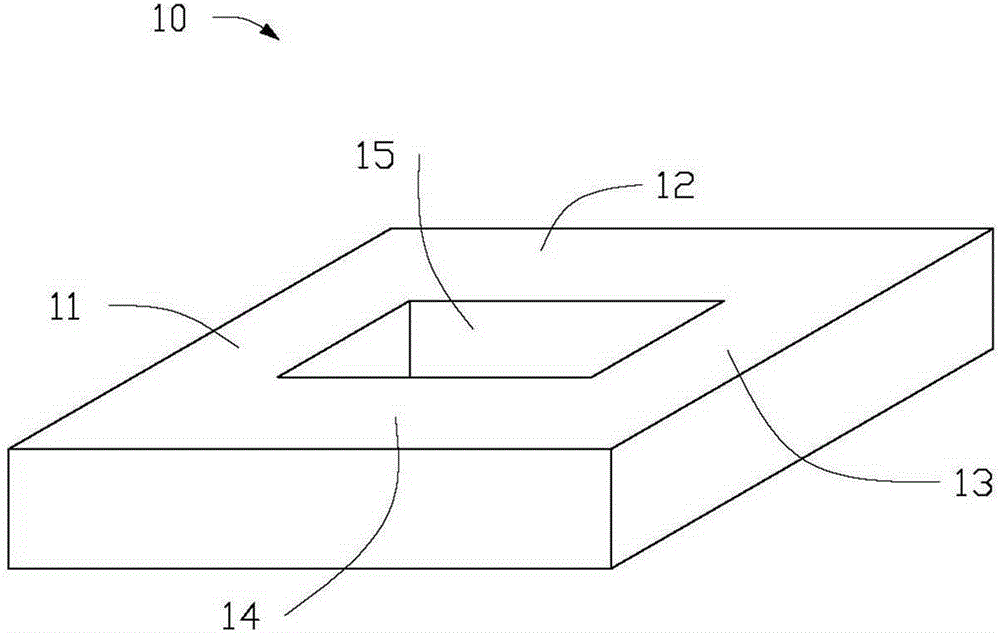
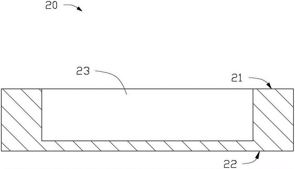
[0044] For a first step, see Figure 1~5 , providing a ferrite 10 and a base layer 20 , and housing the ferrite 10 in the base layer 20 .

[0045] see Figure 1~2 , in this embodiment, the ferrite body 10 is in the shape of a back shape as a whole, and the ferrite body 10 includes a first part 11, a second part 12, a third part 13, a fourth part 14 and a through Groove 15, the first part 11, the second part 12, the third part 13 and the fourth part 14 are sequentially connected, the first part 11 is opposite to the third part 13, the second part 12 is opposite to the The fourth portion 14 is opposite, and the...


PUM


Abstract

The invention relates to a flexible circuit board. The flexible circuit board comprises a base material layer, ferrite contained in the base material layer, a first conductive line layer, a second conductive line layer and a plurality of conductive holes, wherein the first conductive line layer and the second conductive line layer are formed at two surfaces of the base material layer which face opposite directions; the first conductive line layer includes a plurality of first inductance lines; the second conductive line layer includes a plurality of second inductance lines; the conductive holes are electrically connected with the first inductance lines and the second inductance lines; one first inductance lines and one second inductance line which are corresponding to each other, and two conductive holes form an inductance coil; and the plurality of inductance coils are sequentially wound on the ferrite. The present invention also relates to an inductance structure and a fabrication method of the flexible circuit board.

Description

technical field [0001] The invention relates to an inductance structure, a flexible circuit board and a manufacturing method thereof. Background technique [0002] Electronic products have higher and higher requirements in terms of lightness, thinness and high speed. At this stage, for the embedded component technology of the circuit board, the industry has developed a variety of methods for embedding capacitors and resistor materials. However, due to the special structure of the inductor, the circuit The embedded inductor in the board is still made by embedding the entire inductor structure in the substrate layer of the circuit board. The thickness of the circuit board with embedded inductance structure produced by this method is relatively large, which is not conducive to the development of thinner modern electronic products. Contents of the invention [0003] In view of this, the present invention provides a light and thin flexible circuit board and a manufacturing met...

Claims


Application Information

Patent Timeline
Patent Type & Authority Applications(China)
IPC IPC(8): H05K1/18H05K1/16H05K3/46
CPCH05K1/165H05K1/185H05K3/46H05K2201/1003
Inventor 胡先钦李艳禄王凯游文信何明展
Owner AVARY HLDG (SHENZHEN) CO LTD
Features
  • R&D
  • Intellectual Property
  • Life Sciences
  • Materials
  • Tech Scout
  • Unparalleled Data Quality
  • Higher Quality Content
  • 60% Fewer Hallucinations
Learn More