SMI interface device debugging apparatus and method

An interface and device technology, applied in the field of debugging devices for SMI interface devices, can solve problems such as limitations, inability to quickly locate faults, and no significant improvement in R&D efficiency, and achieve the effect of quickly locating faults, facilitating debugging, and improving R&D efficiency.

Inactive Publication Date: 2017-04-19
ZTE CORP
View PDF1 Cites 2 Cited by
  • Summary
  • Abstract
  • Description
  • Claims
  • Application Information

AI Technical Summary

Problems solved by technology

This method is suitable for use in the design of a single board, and is used to manage multiple SMI interface devices on the board. However, in practical applications, an additional logic device PLD is generally not added for switching, but the SMI interface is directly used as a power supply. After flat matching, it is hung on the SMI interface bus of the CPU, and the solution described in this patent cannot avoid the complicated program development and cycle in debugging, cannot quickly locate faults, and has no obvious improvement in actual research and development efficiency
[0005] It can be seen that the debugging method of the existing SMI interface device is limited by the development of the CPU debugging program, which not only affects the research and development efficiency of the SMI interface device, but also cannot quickly locate the fault of the SMI interface device in this debugging method

Method used


Image

  • SMI interface device debugging apparatus and method
  • SMI interface device debugging apparatus and method
  • SMI interface device debugging apparatus and method

Examples


Embodiment 1

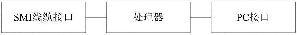
[0038] 本发明实施例提供一种SMI接口器件的调试装置,如 figure 1 所示,所述装置包括:PC接口、处理器、以及SMI线缆接口;其中:

[0039] PC接口,用于接入上位机;

[0040] SMI线缆接口用于接入被调试SMI接口器件;

[0041] 处理器,用于接收通过所述PC接口接入本调试装置的上位机发送的指令,将所述指令转换为SMI格式数据,并将所述SMI格式数据通过模拟的SMI接口发送至通过所述SMI线缆接口连接至本调试装置的被调试SMI接口器件;以及通过模拟的SMI接口接收所述被调试SMI接口器件执行所述指令后反馈的信息,解析该信息,提取出有用信息后将其发送至所述上位机。

[0042] 本实施例中,所述处理器通过将其使用的通信接口一路模拟为时钟信号接口、一路模拟为数据接口的方式,实现对SMI接口的模拟。其中,通信接口包括但不限于为IO接口。

[0043]Further, in this embodiment, the types of instructions sent by the host computer include: a read register instruction and a write register instruction; when the instruction is a read register instruction, the address information of the register is included in the instruction; when the instruction is a write register instruction Instruction, the instruction includes the data written into the register and the address information of the register.

[0044] In a preferred embodiment of the present invention, considering that the types of interfaces supported by the processor may be ...

Embodiment 2

[0055] An embodiment of the present invention provides a debugging device for an SMI interface device. In the debugging device, a single-chip microcomputer system is used as a processor for implementation. Specifically, the debugging device for an SMI interface device described in this embodiment is as follows: figure 2 As shown, including: single-chip microcomputer system, interface conversion chip, PC interface, level matching module, SMI cable interface.

[0056] Among them, the type of the PC interface is usually a USB interface or an RS232 interface, and the PC interface is an external interface for the host computer to connect to the debugging device;

[0057] The interface conversion chip is arranged between the PC interface and the single-chip microcomputer system, which can realize the conversion function from the UART interface supported by the single-chip microcomputer system to the USB / RS232 interface;

[0058] The single-chip microcomputer system, as the core pro...

Embodiment 3

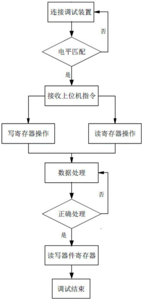
[0087] An embodiment of the present invention provides a debugging method for implementing an SMI interface device using the debugging device described in Embodiment 1 or 2, such as Figure 5 shown, including:

[0088] Step S501, during debugging, the processor converts the instructions of the upper computer imported from the PC interface side into SMI format data;

[0089] In this step, the instruction type of the host computer includes: a read register instruction and a write register instruction;

[0090] When the instruction is a register read instruction, the instruction includes address information of the register; when the instruction is a write register instruction, the instruction includes data written into the register and address information of the register.

[0091] Step S502, the processor sends the SMI format data to the SMI cable interface through the simulated SMI interface, so as to send the SMI format data to the debugged SMI interface device through the SMI...


PUM


Abstract

The invention discloses an SMI (Serial Management Interface) interface device debugging apparatus and method. The debugging apparatus includes a PC interface, a processor, and a SMI cable interface; the processor is used for receiving a command sent by an upper computer which accesses the debugging apparatus via the PC interface, converting the command into SMI format data, and sending the SMI format data to an SMI interface device to be debugged which is connected to the debugging apparatus through the SMI cable interface, by a simulated SMI interface; and receiving information which is fed back after the SMI interface device to be debugged executes the command, through the simulated SMI interface, analyzing the information, extracting useful information, and sending the useful information to the upper computer. The SMI interface device debugging apparatus and method can debug the SMI interface device while a CPU control program is not written or the written program has problems, and can improve the research and development efficiency of software.

Description

technical field [0001] 本发明涉及通信技术领域,尤其涉及一种SMI接口器件的调试装置及方法。 Background technique [0002] 随着网络技术的发展及产品IT化演进,在目前的BBU(基带处理单元)及其他的产品中会应用大量的SMI(Serial Management Interface,串行管理接口)接口的器件,如PHY、交换芯片等,通过这些器件实现设备与以太网、光纤网络的高速通信,这些器件均需要进行配置及调试,来确保其正确稳定的工作。 [0003] 目前的调试方式是通过在电路板内与SMI接口的器件连接的CPU来进行控制,需要编写CPU的软件程序来进行处理。这样在调试很多的SMI接口的器件时会因处理CPU及SMI接口器件的寄存器差异而导致编写软件比较复杂,同时也会增加周期,如果调试过程中出现问题还需要修改程序去定位故障点,这会降低开发效率。 [0004] 在中国专利《SMI接口管理方法及可编程逻辑器件》,申请号:CN201310181278,申请日期:2013.05.15中描述了一种可编程逻辑器件PLD,包括:SMI接口寄存器、以及与其相连的SMI接口收发器和译码器;SMI接口寄存器与处理器CPU通过总线相连;SMI接口收发器的SMI接口通过译码器扩展出与被管理的从SMI接口器件数量相同的主SMI接口;每个扩展出的主SMI接口使用PLD的2个I / O管脚,每个主SMI接口与一个从SMI接口器件相连;不同电平应用的主SMI接口位于PLD的输入输出端口I / O组不同的逻辑区域BANK中,每个BANK的I / O管脚设置成与该BANK内主SMI接口的电平相同的电平模式。这种方法适用于单板内设计时使用,用来进行板内的多片SMI接口器件管理,但实际应用中一般不会额外增加逻辑器件PLD来进行转接,而是直接将SMI接口做电平匹配后挂在CPU的SMI接口总线上,并且该专利所述的方案不能避免调试中的复杂的程序开发及周期,不能快速定位故障,在实际的研发效率上没有明显提升。 [0005] 可见,现有的SMI接口器件的调试方式受限于CPU调试程序的开发,不仅影响SMI接口器件研发效率,而且在该调试方式还不能快速定位SMI接口器件的故障。 Contents of the invention [0006] 鉴于上...

Claims


Application Information

Patent Timeline
IPC IPC(8): G06F13/38
CPCG06F13/38G06F13/385G06F2213/3852
Inventor 付玉堂段向阳封葳庞辉王雪松王文静黄翔黄瑞华王玺曾凯平
Owner ZTE CORP
Why Eureka
Try Eureka