Resistive random access memory device

A resistive random access memory technology, applied in electrical components and other directions, can solve problems such as failure of RRAM devices

Inactive Publication Date: 2017-05-03
WINBOND ELECTRONICS CORP
View PDF9 Cites 5 Cited by
  • Summary
  • Abstract
  • Description
  • Claims
  • Application Information

AI Technical Summary

Problems solved by technology

[0005] The resistive random access memory device of the embodiment of the present invention can overcome the problem in the prior art that when the write voltage is applied to the RRAM device, the oxygen atoms in the resistance transition layer may diffuse back into the resistance transition layer, or even escape. The failure of RRAM devices caused by the top electrode

Method used


Image

  • Resistive random access memory device
  • Resistive random access memory device

Examples


Embodiment Construction

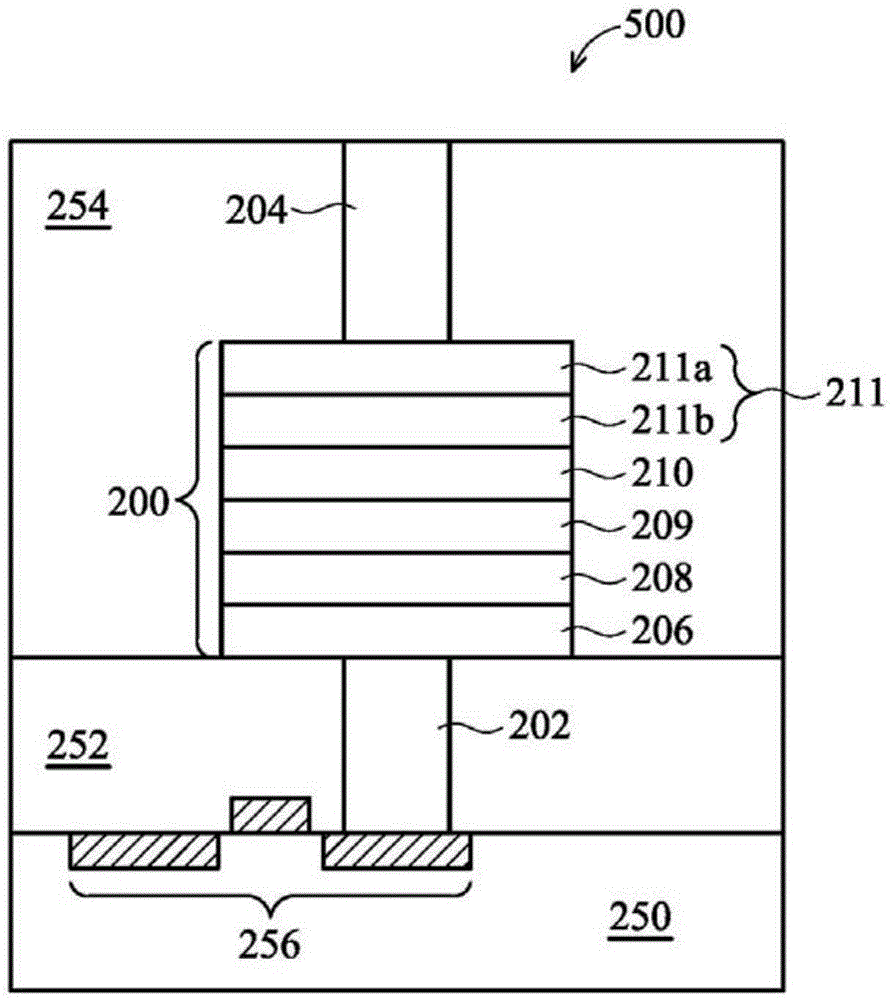
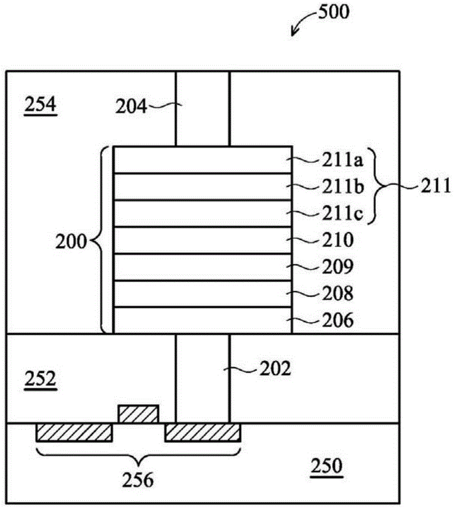
[0023] One embodiment of the present invention provides a non-volatile memory such as a resistive random access memory (RRAM) device. In known RRAM devices, oxygen that migrates from the resistive transition layer into the top electrode due to the applied voltage may diffuse back down to the resistive transition layer, or escape upwards out of the top electrode. The phenomenon of oxygen diffusion / escape in the top electrode described above can render the RRAM device ineffective. To overcome the above oxygen diffusion / escape problem, the present invention provides a novel RRAM stack structure.

[0024] figure 1 It is a cross-sectional view of an RRAM device 500 in an embodiment of the present invention. Such as figure 1 As shown, the RRAM device 500 may be disposed on a semiconductor substrate 250 . In one embodiment, the semiconductor substrate 250 may be a silicon substrate. The main components of the RRAM device 500 include a bottom electrode contact plug 202 disposed o...


PUM


Abstract

A resistive random access memory device is provided, which includes a bottom electrode, a resistive switching layer disposed on the bottom electrode, an oxidizable layer disposed on the resistive switching layer, a first oxygen diffusion barrier layer disposed between the oxidizable layer and the resistive switching layer, and a second oxygen diffusion barrier layer disposed on the oxidizable layer.

Description

technical field [0001] The present invention relates to resistive random access memory (RRAM) devices, and more particularly to stacked structures of RRAM devices. Background technique [0002] A resistive random access memory (RRAM) device has low power consumption, low operating voltage, short write and erase time, long endurance, long storage time, non-destructive read, multi-state storage, simple element process, and Miniaturization and other advantages, so become the mainstream of emerging non-volatile memory. The basic structure of the RRAM device is a metal-insulator-metal (metal-insulator-metal, MIM) stack structure composed of a bottom electrode, a resistive transition layer, and a top electrode, and the resistive switching (RS) resistance of the RRAM device is Value properties are important properties of components. For example, when a write voltage is applied to the RRAM device, the oxygen atoms in the resistance transition layer will migrate to the top electrod...

Claims


Application Information

Patent Timeline
Patent Type & Authority Applications(China)
IPC IPC(8): H01L45/00
CPCH10N70/24H10N70/20H10N70/801H10N70/841H10N70/826H10N70/8833H10N70/828
Inventor 陈达廖绍憬王炳琨
Owner WINBOND ELECTRONICS CORP
Why Eureka
Try Eureka