Display substrate and detection method thereof, display panel and display apparatus

A technology of display substrate and display area, applied in static indicators, instruments, electrical components, etc., can solve the problem of inability to effectively detect the panel packaging effect.

Active Publication Date: 2018-10-12
BOE TECH GRP CO LTD +1
View PDF3 Cites 6 Cited by
  • Summary
  • Abstract
  • Description
  • Claims
  • Application Information

AI Technical Summary

Problems solved by technology

[0005] The present invention provides a display substrate and its detection method, a display panel and a display device to solve the problem that the packaging effect of the display panel cannot be effectively detected

Method used


Image

  • Display substrate and detection method thereof, display panel and display apparatus
  • Display substrate and detection method thereof, display panel and display apparatus
  • Display substrate and detection method thereof, display panel and display apparatus

Examples


Embodiment Construction

[0030] Display products in the prior art use a large number of semiconductor devices, such as: thin film transistors, organic electroluminescent diodes, and water vapor and oxygen will seriously affect the performance and life of these semiconductor devices. Therefore, high demands are placed on the packaging of display products. However, in the prior art, there is no means for detecting the packaging effect. Only when the semiconductor fails, causing the display product to fail to work, can it be found that the packaging effect is not good, causing huge losses.

[0031] In order to solve the above technical problems, the present invention provides a display substrate for providing a means capable of detecting the packaging effect.

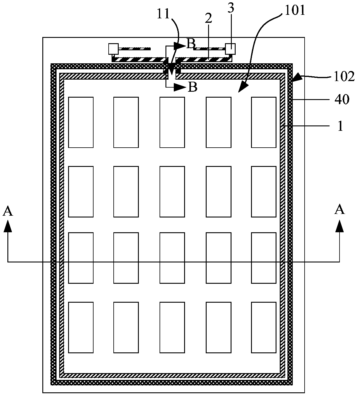
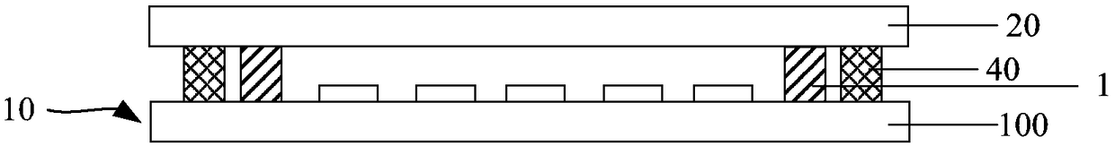
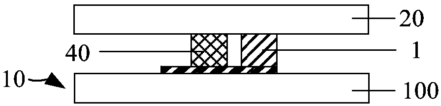
[0032] The display substrate includes a display area and a non-display area located at the periphery of the display area, the non-display area including an encapsulation area. The display substrate further includes a resistive layer pattern, and ...


PUM


Abstract

The invention relates to the technical field of display, and discloses a display substrate and a detection method thereof, a display panel and a display apparatus. A resistor layer pattern is arrangedon one side, close to the center of the display substrate, of a packaging region of the display substrate; the resistor layer pattern selects a hygristor material, so that whether vapor transmits thepackaging region to enter the display region or not can be sensed; and the first ends of two conductive wires are positioned on the outer side, deviated from the display region, of the packaging region, and the second ends of the two conductive wires are electrically connected with the two ends of the resistor layer pattern respectively, so that the resistance value of the resistor layer patterncan be obtained from the parts, positioned on the periphery of the packaging region, of the two conductive wires in the manufacturing process and after manufacturing of the display product, thereby realizing detection of the packaging effect, performing corresponding processing in time, and overcoming the problems of influence to the service life of the display product or even caused failure of the display product caused by a poor packaging effect.

Description

technical field [0001] The present invention relates to the field of display technology, and in particular, to a display substrate and a detection method thereof, a display panel and a display device. Background technique [0002] The organic electroluminescent diode (OLED) display device is a new display technology, its display quality can be compared with thin film transistor active drive liquid crystal display (TFT-LCD), and the price is far lower than it, it will be widely used. LCD technology challenges. Organic electroluminescent devices have the characteristics of high brightness, wide viewing angle, active light emission, high contrast, ultra-thin, portable, etc. Generation Display Technology. [0003] Studies have shown that components such as water vapor and oxygen in the air have a great influence on the life of OLEDs. The reasons are mainly considered from the following aspects: OLEDs need to inject electrons from the cathode during operation, which requires th...

Claims


Application Information

Patent Timeline
IPC IPC(8): H01L27/32H01L51/52G09G3/00
CPCG09G3/006H10K59/12H10K50/84
Inventor 余超智
Owner BOE TECH GRP CO LTD
Why Eureka
Try Eureka