
Pixel structure and liquid crystal display panel

A liquid crystal display panel and pixel structure technology, which is applied in the direction of instruments, nonlinear optics, optics, etc., can solve the problems of user perception impact, deviation, difference, etc., and achieve the effect of improving the phenomenon of large-view role shift and compensating for color shift

Active Publication Date: 2017-05-10
WUHAN CHINA STAR OPTOELECTRONICS TECH CO LTD
View PDF6 Cites 6 Cited by
  • Summary
  • Abstract
  • Description
  • Claims
  • Application Information

AI Technical Summary

Problems solved by technology

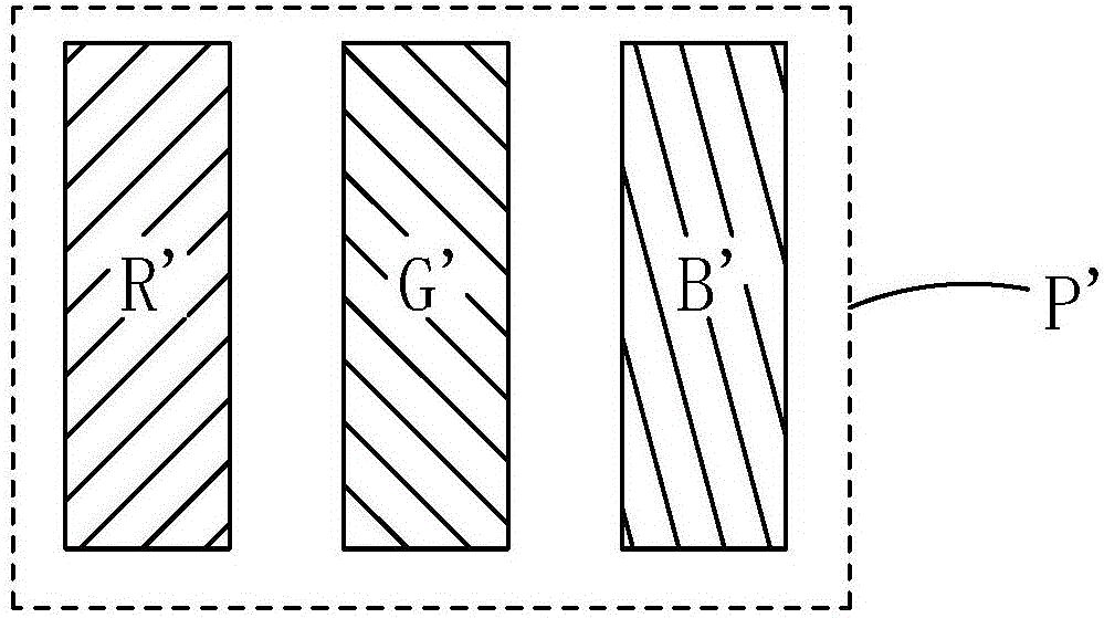
At present, due to the photoelectric characteristics of liquid crystal itself (such as the relatively large difference in the birefringence of liquid crystal molecules) and the combination of materials, the use of the above-mentioned traditional pixel structure will lead to color shift (Color Shift) phenomenon at large viewing angles, that is, in When observing the liquid crystal display panel with the eyes is not facing up, and when the viewing angle is large, the actual viewed color will deviate from the displayed color
Large viewing angles can easily cause chromatic aberration, which will affect the perception of users and affect the quality of products for panel manufacturers
[0005] Reducing color shift is a requirement for the development of liquid crystal display panels, but it is difficult to solve the problem of large-screen color shift through process adjustment in existing technologies

Method used


Image

  • Pixel structure and liquid crystal display panel
  • Pixel structure and liquid crystal display panel
  • Pixel structure and liquid crystal display panel

Examples


Embodiment Construction

[0026] In order to further illustrate the technical means adopted by the present invention and its effects, the following describes in detail in conjunction with preferred embodiments of the present invention and accompanying drawings.

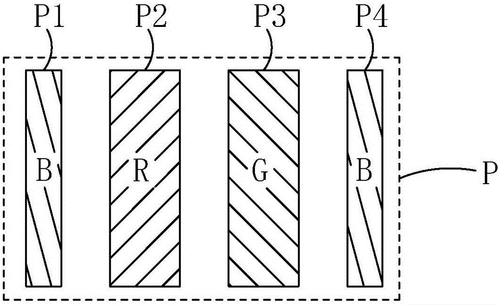
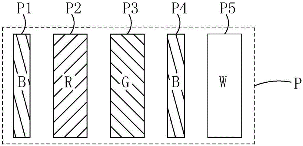
[0027] The present invention firstly provides a pixel structure. figure 2 Shown is the first embodiment of the pixel structure of the present invention, which includes a plurality of pixel units P arranged in an array, and each pixel unit P includes first sub-pixels P1, second sub-pixels P2, The third sub-pixel P3 and the fourth sub-pixel P4. The first sub-pixel P1 and the fourth sub-pixel P4 are respectively arranged on both sides of the second sub-pixel P2 and the third sub-pixel P3; the color resistance colors of the first sub-pixel P1 and the fourth sub-pixel P4 The same, both are blue B; the color resistance color of the second sub-pixel P2 is red R, and the color resistance color of the third sub-pixel P3 is green G; the areas of the s...


PUM


Abstract

The invention provides a pixel structure and a liquid crystal display panel. According to a color principle, a first sub-pixel (P1), a second sub-pixel (P2), a third sub-pixel (P3) and a fourth sub-pixel (P5) orderly arrayed along a straight line are disposed in each pixel unit of the pixel structure, wherein the first sub-pixel (P1) and the fourth sub-pixel (P4) are arranged on two sides of the second sub-pixel (P2) and the third sub-pixel (P3); the area of the second sub-pixel (P2) and the third sub-pixel (P3) are the same; a color resistance color of the first sub-pixel (P1) and the fourth sub-pixel (P4) are the same; the areas of the first sub-pixel (P1) and the fourth sub-pixel (P4) are half of the area of the second sub-pixel (P2); and the color resistance color of the first sub-pixel (P1) and the fourth sub-pixel (P4) are designated to be opposite colors of color cast, so color supplement and correction can be achieved; and color cast of different angle of views can be made up and large angle of view color cast can be improved.

Description

technical field [0001] The invention relates to the field of display technology, in particular to a pixel structure and a liquid crystal display panel. Background technique [0002] A Liquid Crystal Display (LCD) has many advantages such as a thin body, power saving, and no radiation, and has been widely used. Such as: LCD TV, mobile phone, personal digital assistant (PDA), digital camera, computer screen or notebook computer screen, etc., occupy a dominant position in the field of flat panel display. [0003] Most of the liquid crystal displays currently on the market are backlight liquid crystal displays, which include a housing, a liquid crystal display panel disposed in the housing, and a backlight module disposed in the housing. Generally, a liquid crystal display panel is composed of a color filter substrate (ColorFilter, CF), a thin film transistor array substrate (Thin Film Transistor Array Substrate, TFTArray Substrate), and a liquid crystal layer (Liquid Crystal L...

Claims


Application Information

Patent Timeline
Patent Type & Authority Applications(China)
IPC IPC(8): G02F1/1343
CPCG02F1/134309G02F1/133514G02F2201/52G02F1/134345
Inventor 赵凯祥
Owner WUHAN CHINA STAR OPTOELECTRONICS TECH CO LTD
Learn More