Array substrate and display device

A technology of array substrate and cell-matching substrate, applied in the field of liquid crystal display

Active Publication Date: 2014-03-26
BOE TECH GRP CO LTD +1
View PDF3 Cites 19 Cited by
  • Summary
  • Abstract
  • Description
  • Claims
  • Application Information

AI Technical Summary

Problems solved by technology

[0007] The technical problem solved by the embodiments of the present invention is: how to provide an array substrate and a display device, which can effectively solve the problem of improving color shift and achieve the purpose of wide viewing angle at the same time

Method used


Image

  • Array substrate and display device
  • Array substrate and display device
  • Array substrate and display device

Examples


Embodiment 1

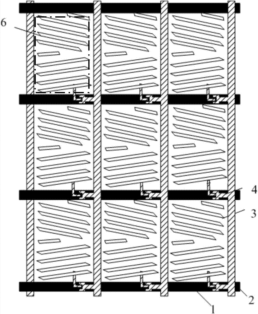
[0038] An embodiment of the present invention provides an array substrate, such as figure 2 As shown, it includes several gate lines 1, data lines 2, and an array of a plurality of network cells formed by the gate lines 1 and data lines 2, and each of the network cells includes: thin film transistors 4 and 4 domains with the same direction The sub-pixel electrodes 3 of the sub-pixel electrodes 3, the thin-film transistor 4 is connected to one of the sub-pixel electrodes 3, the domain orientations of the four sub-pixel electrodes in each network cell are the same, and in each row and column, the domains of two adjacent network cells Oriented into mirror symmetry;

[0039] With the intersection of the gate line 1 and the data line 2 as the center point, the four sub-pixel electrodes 3 adjacent to the center point in the four different network cells adjacent to the center and the crystals controlling the four sub-pixel electrodes 3 The thin-film tube 4 forms a pixel unit; the dom...

Embodiment 2

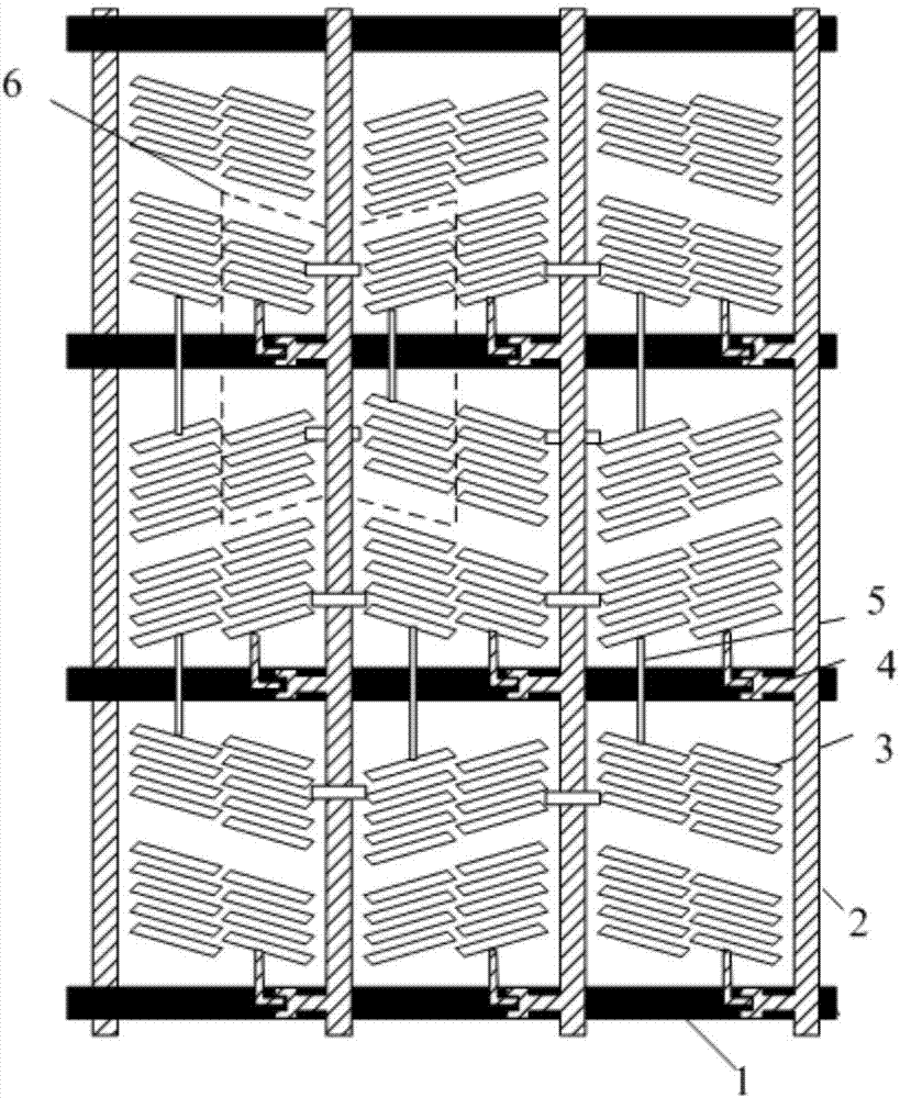
[0045] Compared with embodiment 1, the difference only lies in: as image 3 As shown, the four sub-pixel electrodes 3 in the pixel unit 6 of this embodiment can also be connected through the transparent electrode / ITO via metal connection 5 .

Embodiment 3

[0047] Compared with embodiment 1, the difference only lies in: as Figure 4 As shown, the pixel unit 6 in this embodiment includes two thin film transistors 4 , and each thin film transistor 4 is respectively connected to two sub-pixel electrodes through a TFT connection 5 .


PUM


Abstract

The invention provides an array substrate and a display device, and belongs to the field of liquid crystal display. The array substrate comprises a plurality of grid lines, data lines and an array of a plurality of network unit grids formed by the grid lines and the data lines; each network unit grid comprises at least one thin film transistor and four sub-pixel electrodes in the same domain direction; the intersection points of the grid lines and the data lines serve as center points, and a pixel unit is formed by the four sub-pixel electrodes, adjacent to the center points, coming from the interiors of four different network unit grids with the adjacent centers and thin film transistors for controlling the four sub-pixel electrodes; the four sub-pixel electrodes in the pixel unit are different in domain direction, and are in mirror symmetry distribution in the upper direction, the lower direction, the left direction and the right direction. The uniquely-distributed sub-pixel electrode structure connected with the thin film transistors is driven by the thin film transistors, the wide visual angle effect is even and stable, and the image display quality is improved.

Description

technical field [0001] The invention relates to liquid crystal display technology, in particular to an array substrate and a display device. Background technique [0002] With the rapid development of liquid crystal display technology, people have higher and higher requirements for liquid crystal display. In order to achieve the purpose of wide viewing angle, there are more and more technologies used to realize pixel multi-domain design and mirror symmetry. [0003] For ADS, IPS, VA and other modes, such as figure 1 As shown, it is an array substrate provided in the prior art, which includes a network cell formed by crossing gate lines 1 and data lines 2, and the sub-pixel electrodes in the network cell have a double-domain structure, and the thin film transistor 4 drives the thin film transistor. Network cells (pixel units), so as to achieve the purpose of wide viewing angle. [0004] Among them, ADS is the core technology of planar electric field wide viewing angle - Adv...

Claims


Application Information

Patent Timeline
Patent Type & Authority Applications(China)
IPC IPC(8): G02F1/1362G02F1/1368G02F1/1343
CPCG02F1/133707G02F1/134309G02F1/134363G02F1/1362G02F1/13624G02F1/136286G02F1/134345G02F1/136209G02F1/136227G02F1/1368H01L27/124
Inventor 刘陈曦邵喜斌赵峰
Owner BOE TECH GRP CO LTD
Why Eureka
Try Eureka