Pixel structure, array substrate and display panel
A pixel structure and main pixel technology, applied in static indicators, instruments, nonlinear optics, etc., can solve the problems of potential difference between main pixel unit 1 and sub-pixel unit 2, display panel transmittance and contrast decrease, etc.
- Summary
- Abstract
- Description
- Claims
- Application Information
AI Technical Summary
Problems solved by technology
Method used
Image
Examples
Embodiment 1
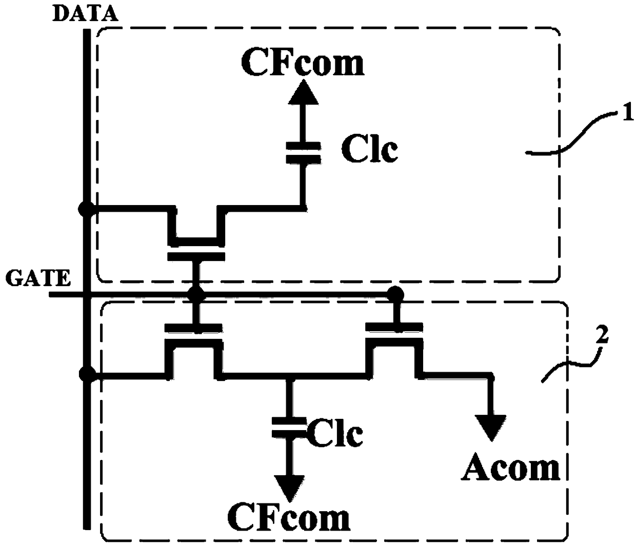
[0037] The pixel structure of the embodiment of the present invention includes a plurality of pixel unit groups. Each pixel unit group includes a plurality of pixel units sequentially arranged along the data line direction. In this embodiment, the scanning lines are arranged along the horizontal direction, and the data lines are arranged along the vertical direction. Each pixel unit includes a main pixel unit 1 and a sub-pixel unit 2 . The main pixel unit 1 and the sub-pixel unit 2 belonging to the same pixel unit are controlled by the same scan line and the same data line.
[0038] Specifically, in one pixel unit, the main pixel unit 1 is configured to receive a scan signal from a scan line, and further receive a data signal from a data line, so as to have a main pixel voltage. The sub-pixel unit 2 is set to receive the scan signal from the same scan line as the main pixel unit 1, and then receive the data signal from the same data line as the main pixel unit 1 and the volt...
Embodiment 2
[0044] In this embodiment, on the basis of the first embodiment, the voltage stabilizing line is optimized.
[0045]In this embodiment, when displaying middle and low gray scale images, the voltage stabilization signal provided by the voltage stabilization line is a DC signal. In addition, the switching element in this embodiment is a thin film transistor.
[0046] In this embodiment, the voltage stabilizing line and the drains of the switching elements of the sub-pixel units 2 of the corresponding pixel unit groups are arranged in the same layer. In this way, the voltage stabilizing line can be directly connected to the drain of the switching element arranged on the same layer without being connected to the drain through a via hole.
[0047] Applying this embodiment, a single patterning process can be used to simultaneously form the voltage stabilizing line and the drain of the switch element, which reduces the manufacturing process steps and difficulty, and improves the man...
Embodiment 3
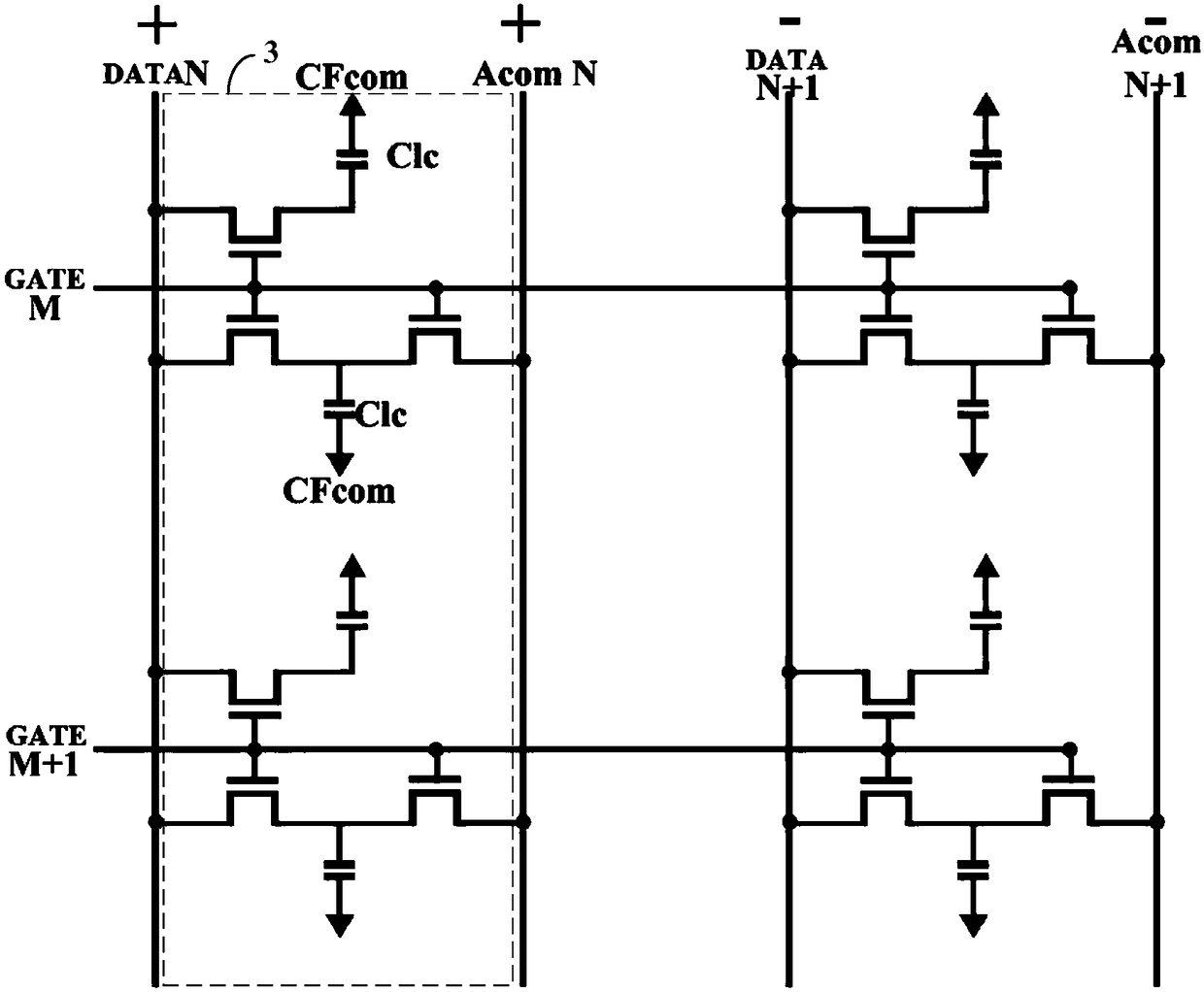
[0050] In this embodiment, a column inversion driving mode (Column Inversion) is used to drive the pixel structure. In the column inversion driving mode, the polarities of the data signals corresponding to two adjacent columns of pixels are opposite, such as figure 2 Indicated by the positive and negative polarity symbols.
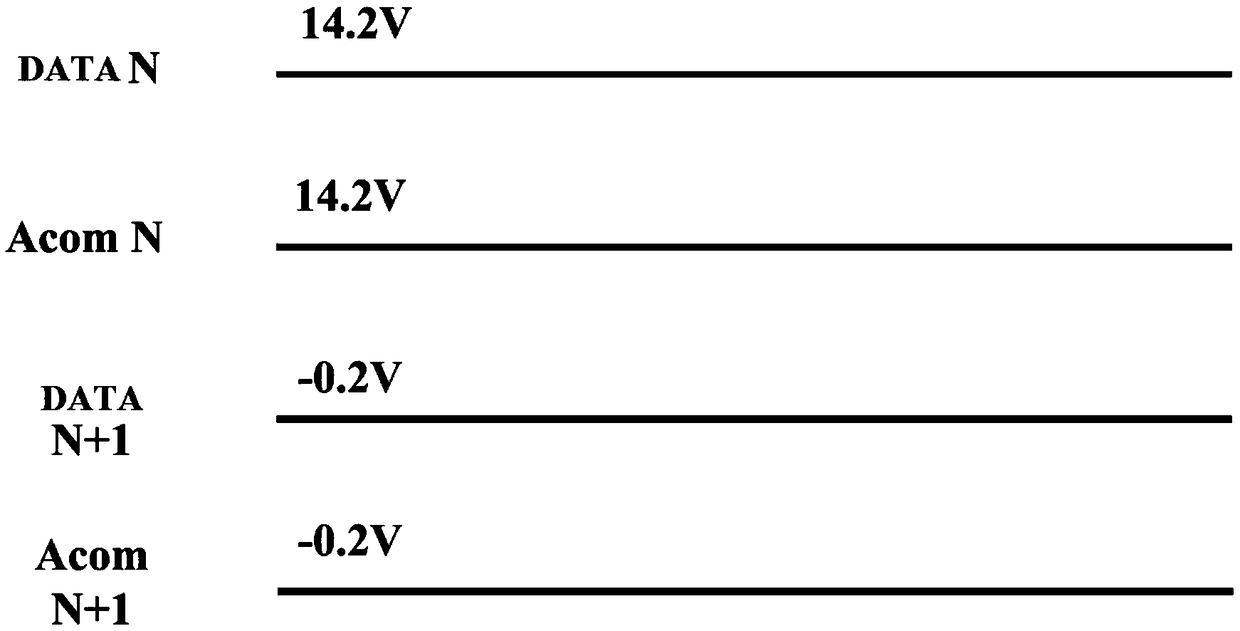
[0051] figure 2 A schematic structural diagram showing a pixel structure in a column inversion driving mode according to an embodiment of the present invention. image 3 shows a frame time for driving figure 2 The driving voltage waveform diagram of the pixel structure shown. refer to figure 2 and image 3 , the scanning lines arranged horizontally are criss-crossed with the data lines arranged vertically and the voltage stabilizing lines arranged vertically. The arrangement of voltage regulator lines is similar to that of data lines. There is no connection between the voltage regulator lines. Each row of voltage stabilizing lines is connected ...
PUM
 Abstract
Description
Claims
Application Information


