Pixel structure, array substrate and display panel

A pixel structure and main pixel technology, applied in static indicators, nonlinear optics, instruments, etc., can solve the problems of potential difference between main pixel unit 1 and sub-pixel unit 2, display panel transmittance and contrast drop, etc.

Active Publication Date: 2017-06-16
TCL CHINA STAR OPTOELECTRONICS TECH CO LTD
View PDF5 Cites 19 Cited by
  • Summary
  • Abstract
  • Description
  • Claims
  • Application Information

AI Technical Summary

Problems solved by technology

However, when using the above-mentioned 3T structure to display middle and low-level images and high-gray-level images, the same voltage-stabilizing signal will always be provided to all voltage-stabilizing lines, which makes there always be a potential difference between the main pixel unit 1 and the sub-pixel unit 2
Therefore, the above-mentioned 3T structure will lead to a decrease in the transmittance and contrast of the display panel when displaying high-gray-scale images

Method used


Image

  • Pixel structure, array substrate and display panel
  • Pixel structure, array substrate and display panel
  • Pixel structure, array substrate and display panel

Examples


Embodiment 1

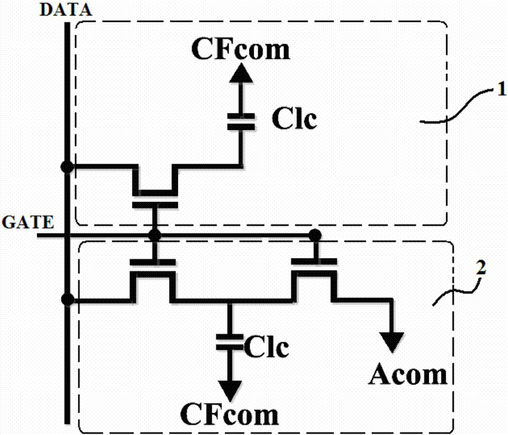
[0037] The pixel structure of the embodiment of the present invention includes a plurality of pixel unit groups. Each pixel unit group includes a plurality of pixel units sequentially arranged along the data line direction. In this embodiment, the scanning lines are arranged along the horizontal direction, and the data lines are arranged along the vertical direction. Each pixel unit includes a main pixel unit 1 and a sub-pixel unit 2 . The main pixel unit 1 and the sub-pixel unit 2 belonging to the same pixel unit are controlled by the same scan line and the same data line.

[0038] Specifically, in one pixel unit, the main pixel unit 1 is configured to receive a scan signal from a scan line, and further receive a data signal from a data line, so as to have a main pixel voltage. The sub-pixel unit 2 is set to receive the scan signal from the same scan line as the main pixel unit 1, and then receive the data signal from the same data line as the main pixel unit 1 and the volt...

Embodiment 2

[0044] In this embodiment, on the basis of the first embodiment, the voltage stabilizing line is optimized.

[0045]In this embodiment, when displaying middle and low gray scale images, the voltage stabilization signal provided by the voltage stabilization line is a DC signal. In addition, the switching element in this embodiment is a thin film transistor.

[0046] In this embodiment, the voltage stabilizing line and the drains of the switching elements of the sub-pixel units 2 of the corresponding pixel unit groups are arranged in the same layer. In this way, the voltage stabilizing line can be directly connected to the drain of the switching element arranged on the same layer without being connected to the drain through a via hole.

[0047] Applying this embodiment, a single patterning process can be used to simultaneously form the voltage stabilizing line and the drain of the switch element, which reduces the manufacturing process steps and difficulty, and improves the man...

Embodiment 3

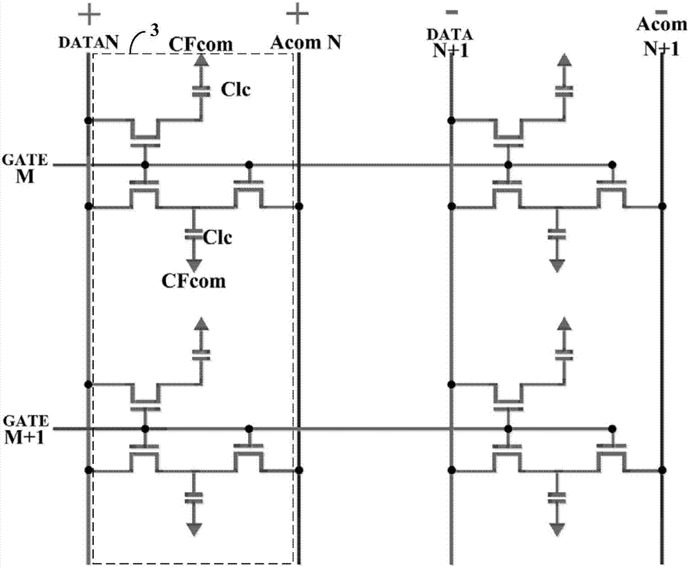
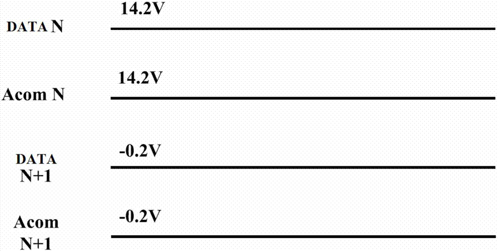
[0050] In this embodiment, a column inversion driving mode (Column Inversion) is used to drive the pixel structure. In the column inversion driving mode, the polarities of the data signals corresponding to two adjacent columns of pixels are opposite, such as figure 2 Indicated by the positive and negative polarity symbols.

[0051] figure 2 A schematic structural diagram showing a pixel structure in a column inversion driving mode according to an embodiment of the present invention. image 3 shows a frame time for driving figure 2 The driving voltage waveform diagram of the pixel structure shown. refer to figure 2 and image 3 , the scanning lines arranged horizontally are criss-crossed with the data lines arranged vertically and the voltage stabilizing lines arranged vertically. The arrangement of voltage regulator lines is similar to that of data lines. There is no connection between the voltage regulator lines. Each row of voltage stabilizing lines is connected ...


PUM


Abstract

The invention discloses a pixel structure, an array substrate and a display panel. The pixel structure comprises a plurality of pixel unit groups, each pixel unit group comprises a plurality of pixel units sequentially arranged in the direction of a data line. Each pixel unit comprises a main pixel unit and a sub-pixel unit. Each pressure-stabilizing line is in one-to-one correspondence with each pixel unit group, and the pressure-stabilizing line is configured to provide pressure-stabilizing signals for each pixel unit in the pixel unit group corresponding to the pressure-stabilizing line. When high gray level images are displayed, the pressure-stabilizing signals provided by the pressure-stabilizing line are the same as data signals received by a currently-opened pixel unit in the pixel unit group corresponding to the pressure-stabilizing line. The gray level brightness of the display panel can be improved under the conditions of displaying the high gray level images, so the light penetration rate and contrast ratio of the display panel are improved, and a large viewing angle compensation function of the display panel can be implemented under the conditions of displaying middle and low gray level images.

Description

technical field [0001] The present invention relates to the technical field of liquid crystal display, in particular to a pixel structure, an array substrate with the pixel structure, and a display panel with the array substrate. Background technique [0002] With the development of liquid crystal display technology, the resolution of liquid crystal displays is getting higher and higher, and the picture quality presented is getting clearer and clearer, while the pixel size is getting smaller and smaller. In order to ensure the picture quality of the display, the pixel design needs to meet higher requirements. In the prior art, a low color shift (Low color) technology is generally used to increase the viewing angle of the display device, so as to achieve a wide viewing angle of the display device. In the prior art, since panel problems such as afterimages are not easy to occur, a low color shift technology is usually implemented by designing a 3T (three TFT) structure. [0...

Claims


Application Information

Patent Timeline
Patent Type & Authority Applications(China)
IPC IPC(8): G02F1/1362G02F1/1368G09G3/36
CPCG02F1/1362G02F1/1368G09G3/3648G02F1/13624G02F1/136286G09G3/3607G09G3/3655G09G3/3696G09G2300/0426G09G2300/0447G09G2300/0809G09G2320/028G09G2320/066G02F1/134345G02F1/133514G02F2203/30G09G2320/0233G09G2320/0673
Inventor 应见见杜鹏
Owner TCL CHINA STAR OPTOELECTRONICS TECH CO LTD
Why Eureka
Try Eureka