Active element array substrate and display panel operation method

A technology of array substrates and active components, applied in nonlinear optics, instruments, optics, etc., to solve problems such as disconnection and inability of pixels to operate

Active Publication Date: 2017-08-29
AU OPTRONICS CORP
View PDF6 Cites 5 Cited by
  • Summary
  • Abstract
  • Description
  • Claims
  • Application Information

AI Technical Summary

Problems solved by technology

Since the scan lines and data lines on the active element array substrate are very long, it is easy to break the line
When the scan line and

Method used


Image

  • Active element array substrate and display panel operation method
  • Active element array substrate and display panel operation method
  • Active element array substrate and display panel operation method

Examples


Embodiment Construction

[0045] Below in conjunction with accompanying drawing, structural principle and working principle of the present invention are specifically described:

[0046] A number of embodiments of the present invention will be disclosed in the following figures. For the sake of clarity, many practical details will be described together in the following description. It should be understood, however, that these practical details should not be used to limit the invention. That is, in some embodiments of the present invention, these practical details are unnecessary. In addition, for the sake of simplifying the drawings, some well-known and commonly used structures and elements will be simply shown in the drawings.

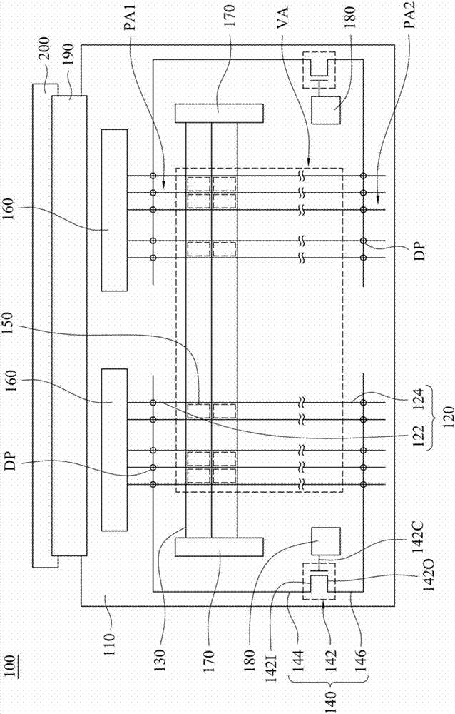
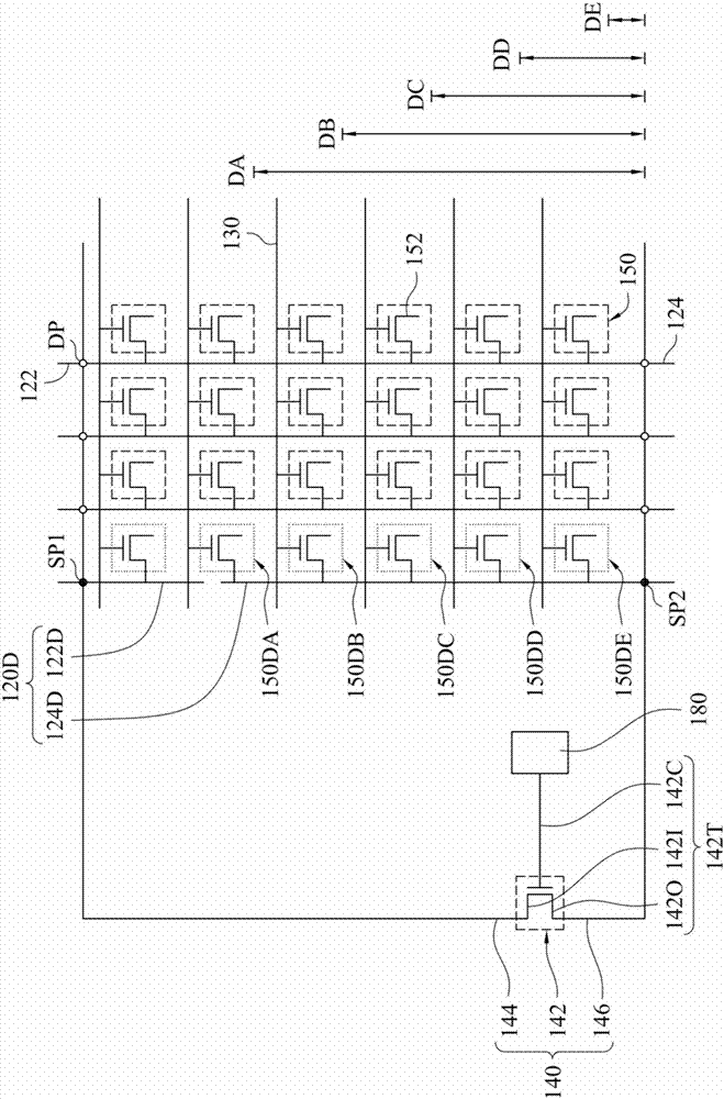
[0047] Figure 1AIt is a schematic top view of the active device array substrate 100 according to some embodiments of the present invention. The active device array substrate 100 includes a substrate 110 , a data line 120 , a scan line 130 , a repair line 140 , a pixel unit 1...


PUM


Abstract

An active element array substrate and display panel operation method is disclosed. An active element array substrate comprises a substrate, a data line, and a repair line. The substrate has a display area, a first peripheral region and a second peripheral region, wherein the first peripheral region and the second peripheral region are respectively provided on opposite sides of the display region. The data line is provided at least in the display area of the substrate and extends to the first peripheral region and the second peripheral region. The repair line comprises at least one impedance modulation circuit, a first repair line segment and a second repair line segment. The impedance modulation circuit has an input terminal, an output terminal and a control terminal, wherein the impedance modulation circuit is used to adjust the impedance according to the control signal received by the control terminal. The first repair line is electrically coupled to the input and extends to the first peripheral region of the substrate. The second repair line is electrically coupled to the output and extends to the second peripheral zone of the substrate.

Description

technical field [0001] The invention relates to an operation method of an active element array substrate and a display panel. Background technique [0002] Generally speaking, a liquid crystal display panel is mainly composed of an active element array substrate, a counter substrate, and a liquid crystal layer sandwiched between the active element array substrate and the opposite substrate, wherein the active element array substrate has a plurality of array arrangements pixels, and each pixel includes an active element and a pixel electrode electrically coupled with the active element. A plurality of scan lines and data lines are arranged on the active device array substrate, and the active device of each pixel is electrically coupled to the corresponding scan line and data line. Since the scan lines and data lines on the active device array substrate are very long, disconnection is likely to occur. When the scan line and the data line are disconnected, some pixels will no...

Claims


Application Information

Patent Timeline
IPC IPC(8): G02F1/1362
CPCG02F1/136259G02F1/136263G02F1/136272
Inventor 谢俊伟潘文哲徐筱菁
Owner AU OPTRONICS CORP
Why Eureka
Try Eureka