Display device and method for manufacturing display device

A technology for a display device and a manufacturing method, which is applied in the manufacturing of semiconductor/solid-state devices, electrical components, circuits, etc., can solve problems such as the reduction of light-emitting characteristics

Inactive Publication Date: 2017-08-29
JAPAN DISPLAY INC
View PDF4 Cites 7 Cited by
  • Summary
  • Abstract
  • Description
  • Claims
  • Application Information

AI Technical Summary

Problems solved by technology

[0003] Here, when the planarization layer is irradiated with ultraviolet rays, the light-emitting element layer provided under

Method used


Image

  • Display device and method for manufacturing display device
  • Display device and method for manufacturing display device
  • Display device and method for manufacturing display device

Examples


Embodiment Construction

[0015] Hereinafter, embodiments of the present invention will be described with reference to the drawings.

[0016] In addition, in the embodiments of the present invention, the expression of arranging other structures "on" a certain structure, when simply expressed as "on", includes the following two unless otherwise specified: A case where another structure is placed directly above a certain structure so as to be in contact with it, and a case where another structure is placed above a certain structure with a third structure interposed therebetween.

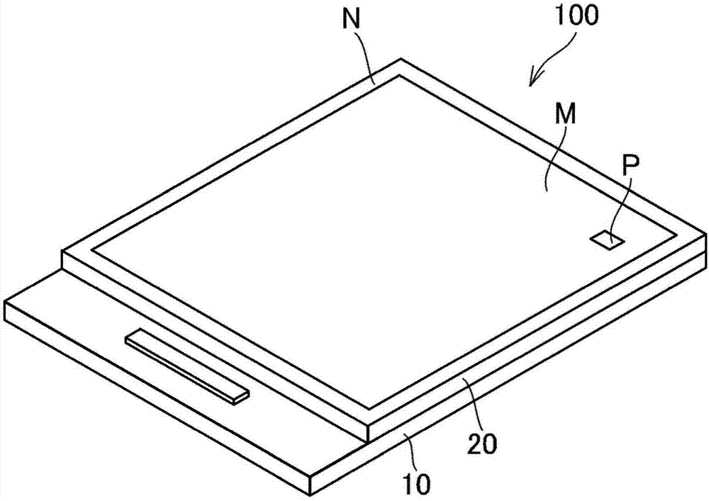
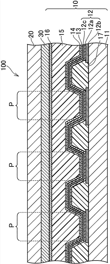
[0017] First, refer to figure 1 , figure 2 , the outline of the overall configuration of the display device according to the first embodiment will be described. figure 1 It is an external perspective view of the display device according to the first embodiment. figure 2 It is a schematic cross-sectional view schematically showing a cross-section of the display device according to the first embodiment. In the first embodim...


PUM


Abstract

The invention relates to a display device and a method for manufacturing the display device. The display device includes a light-emitting element layer that emits light in a way that unit pixels each forming a pixel are respectively controlled in brightness, a sealing layer provided on the light-emitting element layer, an ultraviolet absorbing layer provided on the sealing layer, and a flattening layer provided on the ultraviolet absorbing layer and made of organic resin having ultraviolet curability.

Description

technical field [0001] The present invention relates to a display device and a method for manufacturing the display device. Background technique [0002] Conventionally, a display device is known that includes a light emitting element layer that emits light by controlling luminance of each of a plurality of unit pixels constituting an image, and a sealing layer that covers the light emitting element layer. The sealing layer is provided to prevent the intrusion of moisture from the outside into the device. As a display device having a sealing layer, for example, as disclosed in Japanese Patent Application Laid-Open No. 2013-105947, there is known a display device having a sealing layer formed of an inorganic material, and a sealing layer provided on the sealing layer. A planarization layer formed of an organic resin, and a sealing layer formed of an inorganic material disposed on the planarization layer. The planarization layer is made of ultraviolet curable acrylic resin o...

Claims


Application Information

Patent Timeline
IPC IPC(8): H01L51/52H01L51/50H01L51/56
CPCH10K50/00H10K50/84H10K50/844H10K71/00H10K50/19H10K50/865H10K50/8445H10K2102/00H10K2102/331
Inventor 神谷哲仙大原宏树
Owner JAPAN DISPLAY INC
Why Eureka
Try Eureka