

Semiconductor device
A semiconductor, conductive type technology, applied in the direction of semiconductor lasers, laser parts, electrical components, etc., can solve the problem of large influence of diffusion, and achieve the effect of suppressing the reduction of luminous characteristics
- Summary
- Abstract
- Description
- Claims
- Application Information
AI Technical Summary
Problems solved by technology
Method used
Image

Examples
Embodiment approach 1
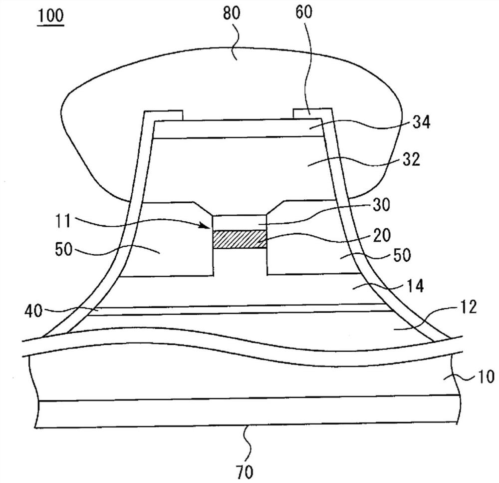
[0021] figure 1 It is a cross-sectional view of the semiconductor device 100 according to the first embodiment. The semiconductor device 100 is an optical semiconductor device such as a semiconductor laser. The semiconductor device 100 is used for optical communication, for example. The semiconductor device 100 includes a semiconductor substrate 10 . An n-type first cladding layer 12 is provided on the semiconductor substrate 10 . An n-type second cladding layer 14 is provided on the first cladding layer 12 . A p-type diffusion suppressing layer 40 is provided between the first cladding layer 12 and the second cladding layer 14 .
[0022] The upper side of the second covering layer 14 is narrower than the lower side. That is, the second cladding layer 14 has a mesa portion. An undoped active layer 20 is provided on the mesa portion of the second cladding layer 14 . A p-type third cladding layer 30 is provided on the active layer 20 . The mesa portion of the second clad...
Embodiment approach 2
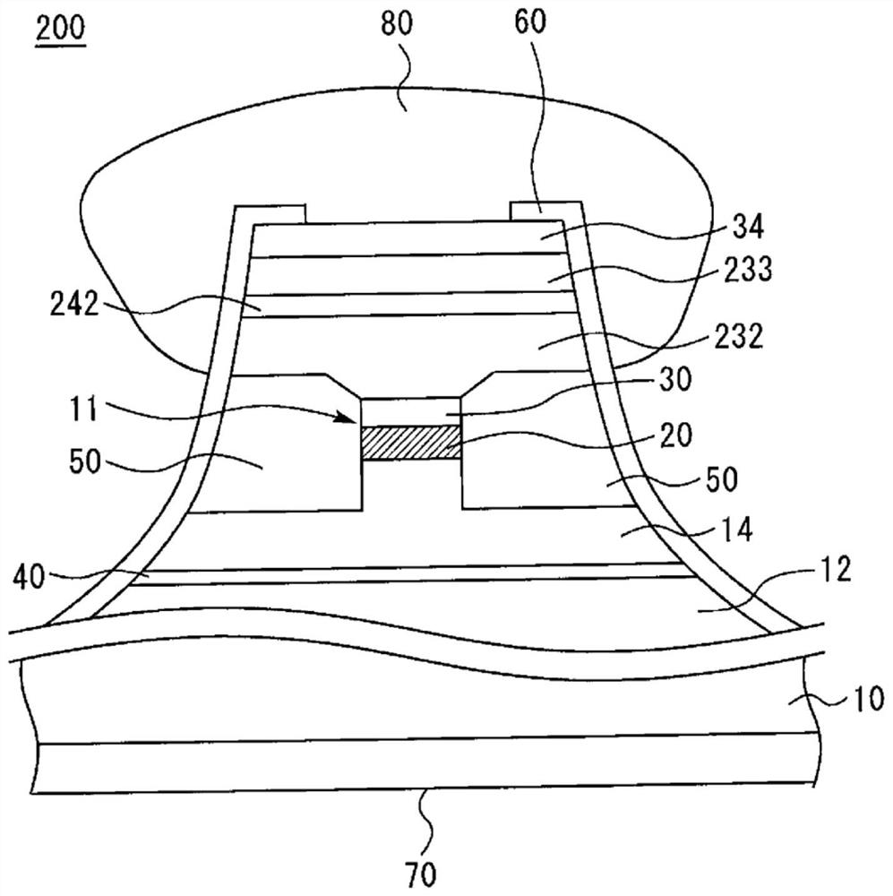
[0055] image 3 It is a cross-sectional view of the semiconductor device 300 according to the second embodiment. Figure 4 Yes image 3 magnified view of . image 3 , 4 An example of a cross section perpendicular to the wave guiding direction of the semiconductor device 300 is shown. The semiconductor device 300 differs from Embodiment 1 in that a diffraction grating layer 340 is provided instead of the diffusion suppressing layer 40 .
[0056] In the semiconductor device 300 , the n-type first cladding layer 312 is provided on the semiconductor substrate 10 . The width of the upper side of the first cladding layer 312 is narrower than that of the lower side. That is, the first cladding layer 312 has a mesa portion. A p-type diffraction grating layer 340 is provided on the mesa portion of the first cladding layer 312 . An n-type second cladding layer 316 is provided on the diffraction grating layer 340 .
[0057] The undoped active layer 20 is provided on the second cl...
Embodiment approach 3
[0070] Figure 5 It is a cross-sectional view of the semiconductor device 400 according to the third embodiment. The present embodiment is characterized in that the active layer 420 is doped.
[0071] In the semiconductor device 400 , the n-type first cladding layer 12 is provided on the semiconductor substrate 10 . The width of the upper side of the first covering layer 12 is narrower than that of the lower side. That is, the first cladding layer 12 has a mesa portion. A p-type active layer 420 is provided on the mesa portion of the first cladding layer 12 . The p-type third cladding layer 30 is provided on the active layer 420 . The mesa portion of the first cladding layer 12 , the active layer 420 , and the third cladding layer 30 form the laminate mesa 11 . The mesa portion of the first cladding layer 12 , the active layer 420 , and the third cladding layer 30 are narrower than the semiconductor substrate 10 in cross-sectional view. Other structures are the same as t...
PUM
| Property | Measurement | Unit |
|---|---|---|
| thickness | aaaaa | aaaaa |
| thickness | aaaaa | aaaaa |
| thickness | aaaaa | aaaaa |
Abstract
Description
Claims
Application Information