
Semiconductor device and manufacturing method of semiconductor device

A manufacturing method and semiconductor technology, which is applied in semiconductor/solid-state device manufacturing, semiconductor devices, semiconductor/solid-state device components, etc., can solve problems such as deterioration of insulation properties, and achieve the effect of suppressing poor insulation

Pending Publication Date: 2021-10-22
MITSUBISHI ELECTRIC CORP
View PDF1 Cites 0 Cited by
  • Summary
  • Abstract
  • Description
  • Claims
  • Application Information

AI Technical Summary

Problems solved by technology

In addition, if air bubbles present in the adhesive reach the circuit pattern, creeping discharge occurs due to the air bubbles, and there is a problem of deterioration of insulation characteristics in semiconductor devices.

Method used


Image

  • Semiconductor device and manufacturing method of semiconductor device
  • Semiconductor device and manufacturing method of semiconductor device
  • Semiconductor device and manufacturing method of semiconductor device

Examples


Embodiment approach 1

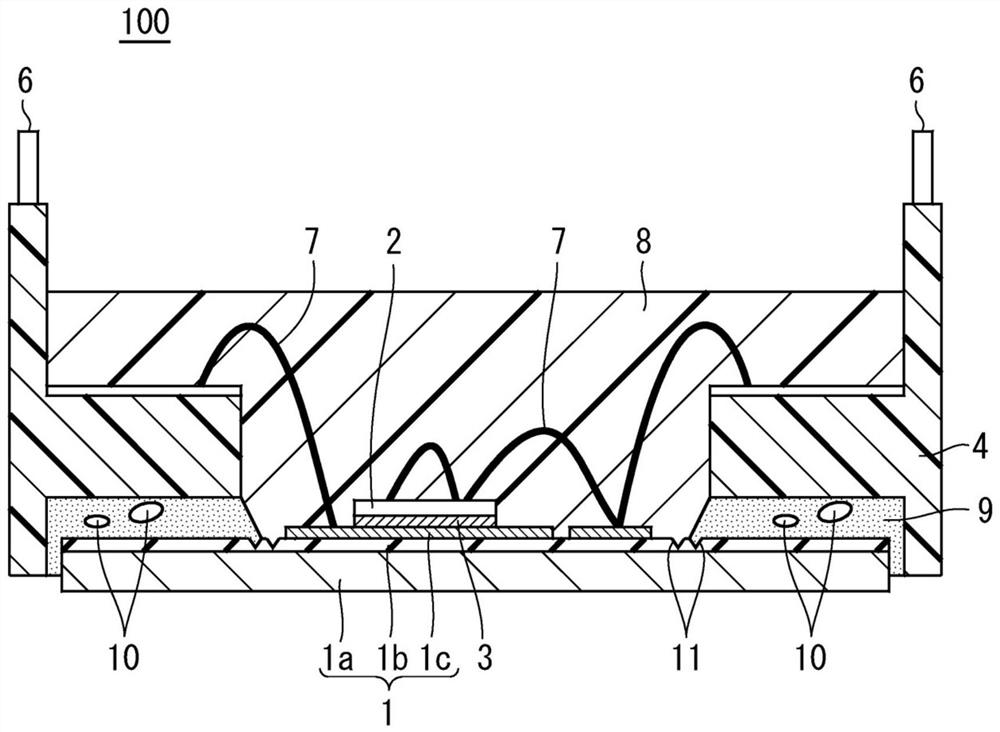
[0015] Hereinafter, Embodiment 1 will be described with reference to the drawings. figure 1 It is a cross-sectional view of the semiconductor device 100 according to the first embodiment.

[0016] like figure 1 As shown, the semiconductor device 100 has a resin-insulated copper base plate 1 , a semiconductor element 2 , a case 4 , electrode terminals 6 , a packaging material 8 , and a roughening pattern 11 .

[0017] The resin-insulated copper base plate 1 has a copper base plate 1a, an insulating layer 1b, and a circuit pattern 1c. The copper base plate 1a, the insulating layer 1b, and the circuit pattern 1c are integrated. The copper base plate 1a is formed in a rectangular shape in plan view. The insulating layer 1b is provided over the entire upper surface of the copper base plate 1a. The insulating layer 1b is made of resin and has a thickness of 0.2 mm. The circuit pattern 1c is provided at a portion other than the outer peripheral portion at the upper surface of th...

Embodiment approach 2

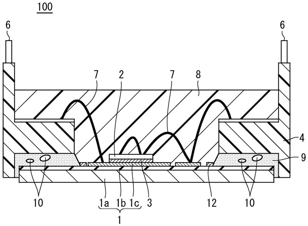
[0031] Next, the semiconductor device 100 according to the second embodiment will be described. figure 2 It is a cross-sectional view of the semiconductor device 100 according to the second embodiment. In addition, in Embodiment 2, the same code|symbol is attached|subjected to the same component as the component demonstrated in Embodiment 1, and description is abbreviate|omitted.

[0032] like figure 2 As shown, in Embodiment 2, instead of the roughening pattern 11 , the semiconductor device 100 has the metal spacer 12 .

[0033] The metal spacer 12 is provided on the upper surface of the insulating layer 1b so as to continuously surround the circuit pattern 1c in a plan view. The metal spacer 12 is made of a metal that can be bonded to the insulating layer 1b, and is formed in a rectangular frame shape in plan view. The metal that can be bonded to the insulating layer 1b is, for example, copper, nickel, aluminum, or the like, but copper is preferable in consideration of ...

Embodiment approach 3

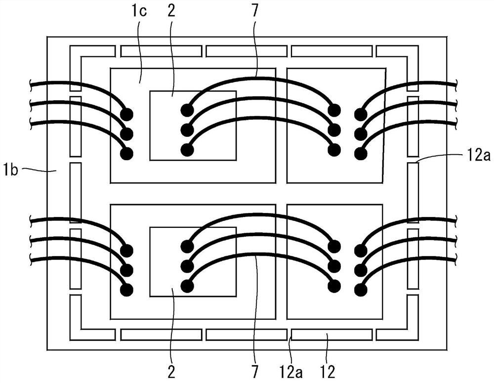
[0042] Next, the semiconductor device 100 according to the third embodiment will be described. image 3 It is a plan view of the resin-insulated copper base plate 1 included in the semiconductor device according to Embodiment 3 and its surroundings. In addition, in Embodiment 3, the same code|symbol is attached|subjected to the same component as the component demonstrated in Embodiment 1, 2, and description is abbreviate|omitted.

[0043] In Embodiment 2, the metal spacer 12 is provided on the upper surface of the insulating layer 1b so as to continuously surround the circuit pattern 1c in plan view, but as image 3 As shown, in Embodiment 3, the metal spacer 12 is provided on the upper surface of the insulating layer 1b so as to surround the circuit pattern 1c intermittently in a plan view. Therefore, gaps 12a are provided in the metal spacer 12 at predetermined intervals.

[0044] When the air bubbles 10 exist in the epoxy resin existing between the circuit pattern 1 c and...


PUM

PropertyMeasurementUnit
widthaaaaaaaaaa
widthaaaaaaaaaa

Abstract

An object is to provide a technique capable of suppressing insulation defects caused by the arrival of bubbles contained in an adhesive at a circuit pattern in a semiconductor device. A semiconductor device (100) includes the resin-insulated copper base plate (1) having the copper base plate (1a), the insulating layer provided on the upper surface of the copper base plate (1a), and the circuit pattern (1c) provided on the upper surface of the insulating layer (1b), the semiconductor element (2) mounted on the upper surface of the resin-insulated copper base plate (1), the case (4) joined to the outer peripheral portion of the resin-insulated copper base plate (1) via the adhesive (9), the sealing material sealing, in the case, the upper surface of the resin-insulated copper base plate and the semiconductor element, and the roughening patterns (11) formed on the upper surface of the insulating layer (1b) such that the circuit pattern (1c) is enclosed therewith in a plan view.

Description

technical field [0001] The present invention relates to a semiconductor device having a resin-insulated copper base plate and a method of manufacturing the same. Background technique [0002] A semiconductor device having a resin-insulated copper base plate, a semiconductor element, and a packaging material is proposed, the resin-insulated copper base plate has a copper base plate, an insulating layer provided on the upper surface of the copper base plate, and an insulating layer on the insulating layer. The circuit pattern set on the surface. The semiconductor element is mounted on the upper surface of the resin-insulated copper base plate. The case is joined to the outer peripheral portion of the resin-insulated copper base plate via an adhesive. The encapsulating material encapsulates the upper surface of the resin-insulated copper base plate and the semiconductor element inside the case (for example, refer to Patent Document 1). [0003] Patent Document 1: Japanese Pa...

Claims


Application Information

Patent Timeline
Patent Type & Authority Applications(China)
IPC IPC(8): H01L23/13H01L23/498H01L23/31H01L21/48
CPCH01L23/13H01L23/49838H01L23/3107H01L21/4846H01L23/053H01L23/142H01L2224/32225H01L2224/45124H01L2224/48227H01L2224/291H01L24/32H01L24/48H01L2224/73265H01L23/10H01L2924/19107H01L2924/00014H01L2924/014H01L2924/00H01L23/3142H01L24/45H01L21/4871H01L23/4924
Inventor 作元祥太朗
Owner MITSUBISHI ELECTRIC CORP
Learn More