Array substrate and display panel
An array substrate and display panel technology, which is applied to static indicators, instruments, identification devices, etc., can solve the problems of display quality degradation of the display panel and excessive data line load, so as to alleviate the excessive brightness of the display, avoid the split screen line, Display the effect of brightness reduction
- Summary
- Abstract
- Description
- Claims
- Application Information
AI Technical Summary
Problems solved by technology
Method used
Image

Examples
Embodiment Construction
[0015] The following will clearly and completely describe the technical solutions in the embodiments of the present invention in conjunction with the accompanying drawings in the embodiments of the present invention. Obviously, the described embodiments are only some of the embodiments of the present invention, not all of them. Based on the embodiments of the present invention, all other embodiments obtained by persons of ordinary skill in the art without making creative efforts belong to the protection scope of the present invention.
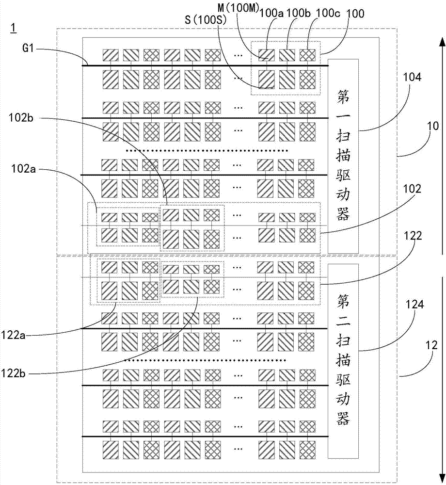
[0016] see figure 1 , figure 1 It is a schematic structural view of an embodiment of the array substrate of the present invention, and the array substrate 1 includes a first display area 10 and a second display area 12 adjacent to each other. In one embodiment, as figure 1 As shown, the array substrate 1 used in the present invention can be in the line scanning split-screen driving mode, that is, the first display area 10 and the second displ...
PUM
 Abstract
Description
Claims
Application Information