
A kind of photoresist etching back planarization method

A flattening method and photoresist technology, applied in optics, optomechanical equipment, instruments, etc., can solve the problems of air expansion, bubbles, and photoresist being easily etched, and achieve the effect of ensuring the degree of flattening

Active Publication Date: 2020-12-04
上海彤程电子材料有限公司 +1
View PDF5 Cites 0 Cited by
  • Summary
  • Abstract
  • Description
  • Claims
  • Application Information

AI Technical Summary

Problems solved by technology

However, in the above process, if there are small gaps on the surface of the dielectric layer, the air in the small gaps tends to expand during the photoresist coating and baking process, which will cause a bubble to form on the surface of the small gaps.
Due to the presence of bubbles, the thickness of the photoresist here will be very small, so the photoresist is easily etched through, and the dielectric layer in the area where the bubbles are located is easily over-etched, and even the dielectric can be damaged. other layers below the layer, resulting in poor planarization

Method used


Image

  • A kind of photoresist etching back planarization method
  • A kind of photoresist etching back planarization method
  • A kind of photoresist etching back planarization method

Examples


Embodiment Construction

[0021] The following will clearly and completely describe the technical solutions in the embodiments of the present invention. Obviously, the described embodiments are only some of the embodiments of the present invention, rather than all the embodiments. Based on the embodiments of the present invention, all other embodiments obtained by persons of ordinary skill in the art without making creative efforts belong to the protection scope of the present invention.

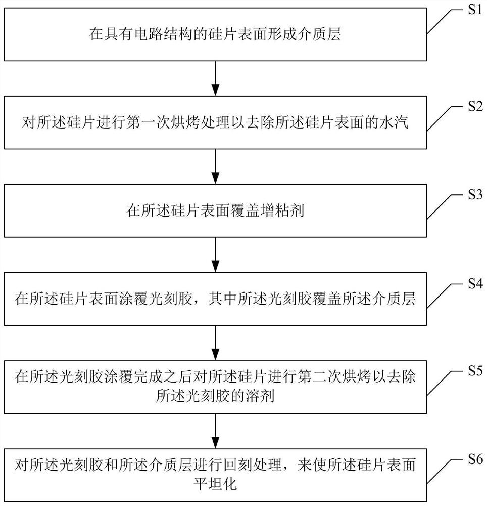
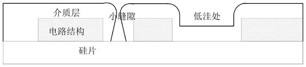
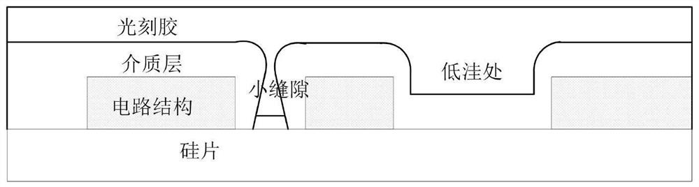
[0022] In order to solve the problem in the prior art that the etching-back planarization effect of the photoresist is poor due to air bubbles during the etching-back process of the photoresist in the semiconductor chip manufacturing process, the invention provides a method for etching-back planarization of the photoresist , which is mainly through the photoresist coating during the natural cooling process of the silicon wafer after the silicon wafer is baked, so that the air in the small gap in the dielectric layer s...


PUM


Abstract

The invention provides a back-etching planarization method for a photoresist. The back-etching planarization method for the photoresist comprises the following steps: forming a dielectric layer on the surface of a silicon wafer with a circuit structure; performing primary roasting treatment on the silicon wafer; in a natural cooling process of the silicon wafer, coating the surface of the silicon wafer with the photoresist, wherein the photoresist covers the dielectric layer; performing secondary roasting treatment on the silicon wafer after the photoresist is coated; and back-etching the photoresist and the dielectric layer to planarize the surface of the silicon wafer. The method provided by the invention can prevent from excessively etching or even damaging other film layers in the planarized etching process of the photoresist, so that the planarizing degree of photoresist back-etching is effectively guaranteed.

Description

【Technical field】 [0001] The invention relates to the technical field of semiconductor chip manufacturing, in particular to a photoresist etching back planarization method. 【Background technique】 [0002] In the manufacturing process of semiconductor chips, photoresist etching back planarization is an important process technology, which mainly uses the photoresist coated on the dielectric layer to etch it, so as to achieve the planarization of the dielectric layer. layer purpose. However, in the above process, if there are small gaps on the surface of the dielectric layer, the air in the small gaps tends to expand during the coating and baking process of the photoresist, which will cause a bubble to form on the surface of the small gaps. Due to the presence of bubbles, the thickness of the photoresist here will be very small, so the photoresist is easily etched through, and the dielectric layer in the area where the bubbles are located is easily over-etched, and even the di...

Claims


Application Information

Patent Timeline
Patent Type & Authority Patents(China)
IPC IPC(8): G03F7/16
CPCG03F7/168
Inventor 魏绍均
Owner 上海彤程电子材料有限公司
Learn More