OLED, OLED drive array and charging method of OLED drive array

A technology for driving arrays and charging methods, applied in instruments, static indicators, etc., can solve problems such as insufficient charging time of pixels or sub-pixels, affecting OLED display brightness, difficulty in balancing the number of source drive channels and charging time, etc. Taking into account the charging time, ensuring the charging time, and reducing the number of effects

Inactive Publication Date: 2017-11-07
芯颖科技有限公司
View PDF8 Cites 0 Cited by
  • Summary
  • Abstract
  • Description
  • Claims
  • Application Information

AI Technical Summary

Problems solved by technology

[0003] In the application of AM OLED (Active Matrix Organic Light Emitting Diode, Active Matrix Organic Light Emitting Diode) to realize FULL HD, usually, each source drive channel in OLED drives a column of pixels or sub-pixels; however, it is limited by the structure of OLED itself , in order to reduce the number of source drive channels, data selector Mux is sometimes used, so that each source drive channel drives two columns of pixels or sub-pixels, so that the charging time of each column of pixels or sub-pixels is reduced by half. Or the sub-pixel charging time is insufficient, which affects the overall display brightness of the OLED
[0004] For the above-mentioned existing OLED driving methods, the number of source driving channels and the charging time are difficult to balance, and no effective solution has been proposed.

Method used


Image

  • OLED, OLED drive array and charging method of OLED drive array
  • OLED, OLED drive array and charging method of OLED drive array
  • OLED, OLED drive array and charging method of OLED drive array

Examples


Embodiment 1

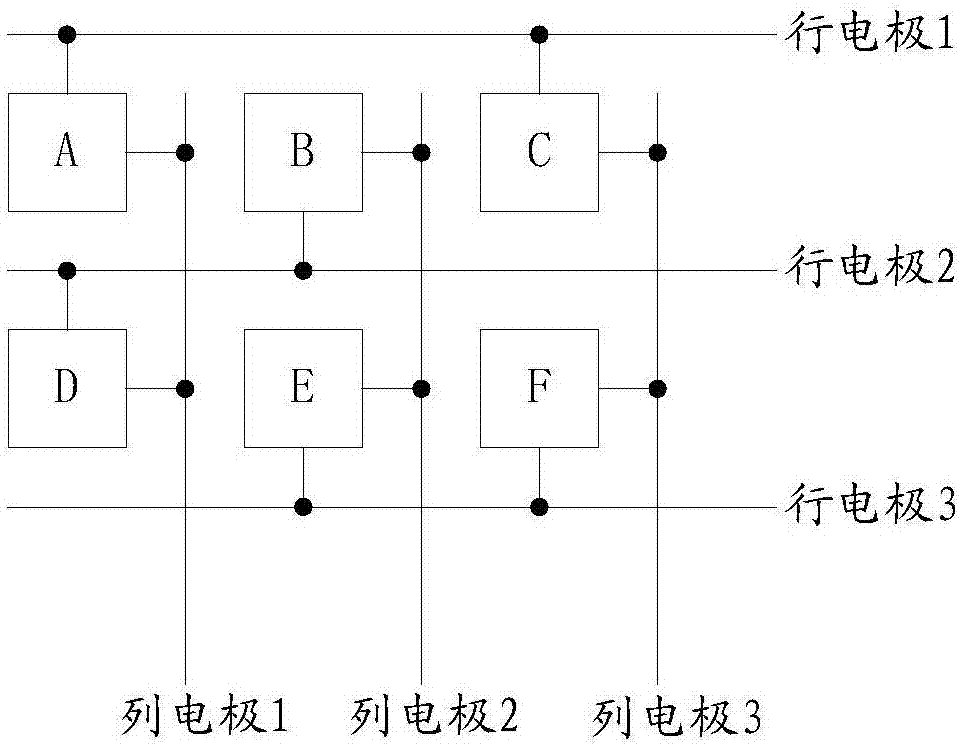
[0031] see figure 1 A schematic diagram of a partial structure of the first OLED drive array shown; multiple pixel rows are set in the OLED drive array; each pixel row includes multiple pixels or sub-pixels;

[0032] Wherein, every two pixel rows are provided with three row electrodes and three column electrodes; in the two pixel rows, each pixel or sub-pixel is connected with one of the row electrodes and one column electrode; the three row electrodes are sequentially arranged according to the set order Turn on: one or more of the three column electrodes are turned on sequentially according to the set combination and sequence, and are used to charge the pixel or sub-pixel.

[0033] figure 1 Taking two pixel rows as an example, each pixel row includes three pixels; wherein, pixel row 1 includes pixels A, B, and C, and pixel row 2 includes pixels D, E, and F; three row electrodes (row electrode 1, row electrode Electrodes 2 and row motors 3) are arranged at intervals of pixel...

Embodiment 2

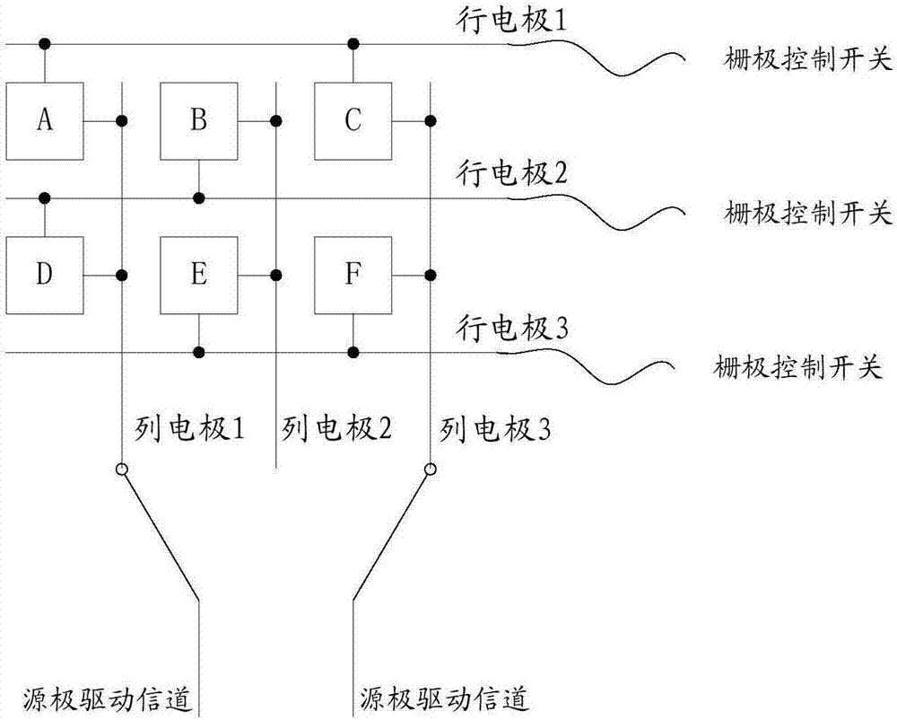
[0040] see figure 2 The partial structural schematic diagram of the second OLED driving array is shown; the OLED driving array is realized on the basis of the OLED driving array provided in the first embodiment.

[0041] The OLED driving array is provided with a plurality of pixel rows; each pixel row contains a plurality of pixels or sub-pixels; wherein, every two pixel rows are provided with three row electrodes and three column electrodes; in two pixel rows, each pixel Or the sub-pixel is connected with one row electrode and one column electrode; the three row electrodes are turned on sequentially according to the set order; one or more electrodes in the three column electrodes are turned on sequentially according to the set combination and order, which is used for the pixel or sub-pixels for charging.

[0042] Further, the above-mentioned row electrodes are connected with a gate control switch (the gate control switch may also be referred to as Gate); the gate control sw...

Embodiment 3

[0052] Corresponding to the OLED driving array provided in the above-mentioned embodiments, see Figure 4 The flowchart of the charging method of a kind of OLED driving array shown; This method is applied to above-mentioned OLED driving array, and this method comprises the steps:

[0053] Step S402, when the first row electrode is turned on, the first and third column electrodes are turned on to charge the corresponding pixels or sub-pixels;

[0054] Step S404, when the second row electrode is turned on, the first and second column electrodes are turned on to charge the corresponding pixels or sub-pixels;

[0055] Step S406, when the third row electrode is turned on, the second and third column electrodes are turned on to charge the corresponding pixels or sub-pixels.

[0056] In actual implementation, the above step S402 to step S406 can be infinitely looped to charge the pixels or sub-pixels multiple times.

[0057] In an OLED drive array provided by an embodiment of the p...


PUM


Abstract

The invention provides an OLED, an OLED drive array and a charging method of the OLED drive array. In the drive array, every two pixel lines are provided with three line electrodes and three column electrodes; each pixel or sub-pixel is connected with one line electrode and one column electrode; the three line electrodes are sequentially started according to a set sequence; one or more of the three column electrodes are sequentially started according to a set combination and sequence and used for charging the pixels or sub-pixels. Every two pixel lines are provided with three line electrodes, there is no need to configure a source electrode drive channel for each line electrode, and the number of source electrode drive channels can be reduced; under the condition that the number of the source drive channels is small, the charging time of each pixel or sub-pixel is guaranteed, then the overall brightness of an OLED display screen and the accuracy of color display of the OLED display screen are guaranteed, and color display deviation and the non-ideal effect of the display screen caused by too short a charging time are avoided.

Description

technical field [0001] The invention relates to the field of display technology, in particular to an OLED, an OLED driving array and a charging method thereof. Background technique [0002] FULL HD (Full High Definition) refers to a display standard with a physical resolution up to 1920×1080, including 1080i and 1080P; among them, i (interlace) stands for interlaced scanning; P (Progressive) stands for progressive scanning; therefore , 1080P has better picture quality and fineness than 1080i. [0003] In the application of AM OLED (Active Matrix Organic Light Emitting Diode, Active Matrix Organic Light Emitting Diode) to realize FULL HD, usually, each source drive channel in OLED drives a column of pixels or sub-pixels; however, it is limited by the structure of OLED itself , in order to reduce the number of source drive channels, data selector Mux is sometimes used, so that each source drive channel drives two columns of pixels or sub-pixels, so that the charging time of e...

Claims


Application Information

Patent Timeline
Patent Type & Authority Applications(China)
IPC IPC(8): G09G3/3208
CPCG09G3/3208
Inventor 蔡宗宪曾德源
Owner 芯颖科技有限公司
Why Eureka
Try Eureka