Mask plate, oled display substrate and manufacturing method thereof, display device

A technology for a display substrate and a manufacturing method, which can be applied to static indicators, patterned surface photoengraving processes, semiconductor/solid-state device manufacturing, etc., can solve problems such as uneven display brightness, improve display quality, and improve display brightness unevenness. effect of the problem

Active Publication Date: 2020-12-01
BOE TECH GRP CO LTD +1
View PDF6 Cites 0 Cited by
  • Summary
  • Abstract
  • Description
  • Claims
  • Application Information

AI Technical Summary

Problems solved by technology

[0004] The technical problem to be solved by the present invention is to provide a mask plate, an OLED display substrate and its manufacturing method, and a display device, which can improve the problem of uneven display brightness of the display device and improve the display quality of the display device

Method used


Image

  • Mask plate, oled display substrate and manufacturing method thereof, display device
  • Mask plate, oled display substrate and manufacturing method thereof, display device
  • Mask plate, oled display substrate and manufacturing method thereof, display device

Examples


Embodiment Construction

[0037] In order to make the technical problems, technical solutions and advantages to be solved by the embodiments of the present invention clearer, the following will describe in detail with reference to the drawings and specific embodiments.

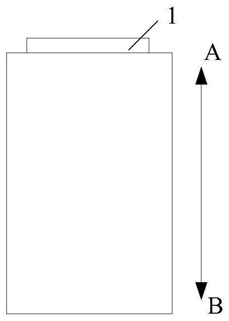
[0038] Such as figure 1 As shown, in the existing OLED display device, IC (driving circuit) 1 inputs Vss signal to the cathode, IC1 inputs Vdd signal to the anode, and the voltage difference between the Vdd signal and the Vss signal is the driving voltage ΔV, which is driven by the driving voltage ΔV The luminescent material emits light.

[0039] Since there is a certain impedance in the data line of the OLED display device, such as figure 1 As shown, in the direction from A to B, there is a certain voltage drop between the Vdd signal at the far end of the IC and the Vdd signal at the near end of the IC, resulting in a difference between the driving voltage ΔV at the far end of the IC and the driving voltage ΔV at the near end of the ...


PUM


Abstract

The invention provides a mask plate, an OLED display substrate, a manufacturing method thereof, and a display device, belonging to the field of display technology. The mask plate includes a plurality of array-arranged openings for making the pattern of the pixel defining layer of the OLED display substrate. The width of the opening of the first side of the mask plate in a first direction, the first direction being a direction from close to the first side of the mask plate to away from the first side edge of the mask plate. The gradient angle of the pattern of the pixel defining layer close to the second side of the OLED display substrate is smaller than the gradient angle of the pattern of the pixel defining layer away from the second side of the OLED display substrate. The technical proposal of the invention can improve the problem of uneven display brightness of the display device and improve the display quality of the display device.

Description

technical field [0001] The invention relates to the field of display technology, in particular to a mask plate, an OLED display substrate, a manufacturing method thereof, and a display device. Background technique [0002] In the existing OLED display device, the Vss signal is input from the IC (driver circuit) to the cathode, and the Vdd signal is input from the IC to the anode. The voltage difference between the Vdd signal and the Vss signal is the driving voltage ΔV, and the luminescent material is driven by the driving voltage ΔV to emit light. . [0003] Due to the certain impedance of the data line of the OLED display device, there is a certain voltage drop between the Vdd signal at the far end of the IC and the Vdd signal at the near end of the IC, resulting in a difference between the driving voltage ΔV at the far end of the IC and the driving voltage ΔV at the near end of the IC. The LRU problem occurs, that is, the long-term display brightness of the OLED display ...

Claims


Application Information

Patent Timeline
Patent Type & Authority Patents(China)
IPC IPC(8): G03F1/64H01L27/32H01L51/56
CPCG03F1/64G09G3/3258H10K59/122H10K71/166H10K77/10H10K50/81H10K50/82H10K50/822H10K71/00H10K2102/351
Inventor 莫再隆阳智勇杨凡周炟
Owner BOE TECH GRP CO LTD
Why Eureka
Try Eureka