Supercharge Your Innovation With Domain-Expert AI Agents!

Display substrate, manufacturing method thereof and display device

A display substrate and substrate technology, which is applied in semiconductor/solid-state device manufacturing, electrical components, electric solid-state devices, etc., can solve the problems of light leakage in display equipment, reduce light leakage, increase lateral transmission paths, and solve the effects of influence

Inactive Publication Date: 2017-11-17
TCL CHINA STAR OPTOELECTRONICS TECH CO LTD
View PDF6 Cites 10 Cited by
  • Summary
  • Abstract
  • Description
  • Claims
  • Application Information

AI Technical Summary

Problems solved by technology

[0003] With the improvement of the resolution of organic light-emitting diode displays, the pitch between the pixels of the display is getting smaller and smaller, which makes the display device prone to light leakage

Method used


Image

  • Display substrate, manufacturing method thereof and display device
  • Display substrate, manufacturing method thereof and display device
  • Display substrate, manufacturing method thereof and display device

Examples


Embodiment Construction

[0017] In order to make the technical problems solved by the present invention, the technical solutions adopted and the technical effects achieved clearer, the technical solutions of the embodiments of the present invention will be further described in detail below in conjunction with the accompanying drawings.

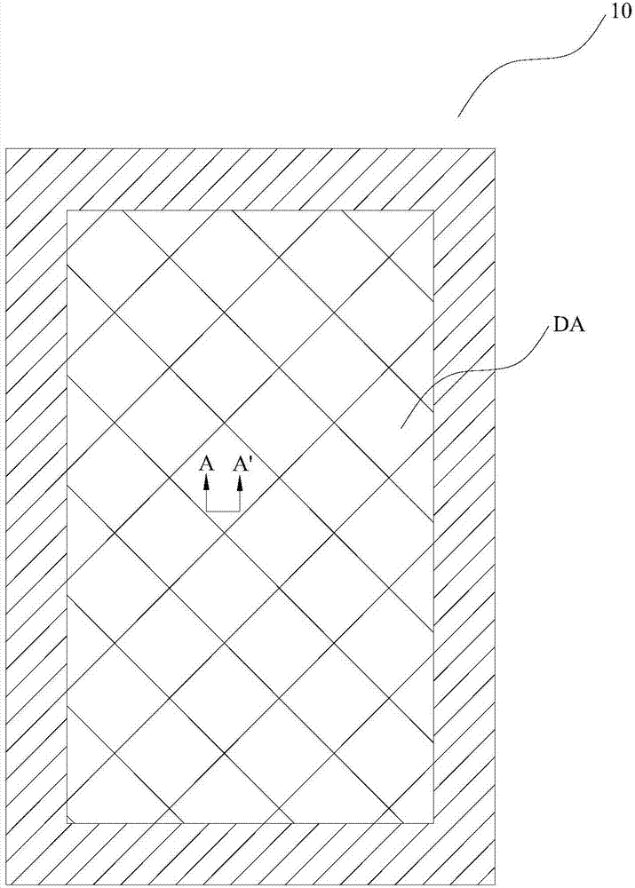
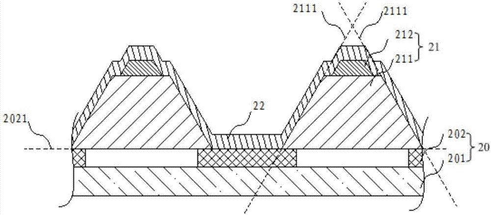
[0018] see figure 1 with figure 2 ,in figure 1 It is a schematic structural view of the display substrate of Embodiment 1, figure 2 yes figure 1 It is a schematic structural diagram showing an embodiment of a cross-section of the substrate along the A-A direction.

[0019] refer to figure 1 The display substrate 10 of this embodiment includes a substrate 20 , a pixel definition layer 21 and an organic light-emitting functional layer 22 , and the light-emitting area DA of the display substrate 10 is set. The substrate 20 includes a glass substrate 201 and an indium tin oxide layer (ITO layer, hereinafter referred to as the ITO layer) 202, and the ITO layer is di...


PUM


Abstract

The invention discloses a display substrate, a manufacturing method thereof and a display device. The display substrate comprises a substrate, a pixel definition layer and an organic light emitting functional layer, and is characterized in that the pixel definition layer defines a plurality of spaced pixel regions and enables the pixel regions to form grooves, and the pixel definition layer comprises a first pixel definition layer and a second pixel definition layer; the first pixel definition layer is arranged at one side of the substrate; the second pixel definition layer is arranged at the side, which is back to the substrate, of the first pixel definition layer; the second pixel definition layer is located between a flat plane / curved plane defined by the side wall of the first pixel definition layer and a flat plane defined by the substrate; and the organic light emitting functional layer covers the surface of the pixel definition layer and fills the grooves formed by the pixel definition layer and the substrate. According to the above scheme, the display substrate can solve or relieve a problem of light leakage of the existing OLED display.

Description

technical field [0001] The invention relates to the field of display equipment, in particular to a display substrate, a manufacturing method thereof, and a display device. Background technique [0002] As more and more organic light-emitting diodes (OLEDs) are used in display devices, the display technology of the organic light-emitting diodes continues to develop towards a high-resolution trend while ensuring the brightness of the display devices. [0003] With the improvement of the resolution of the organic light emitting diode display, the pitch between the pixels of the display is getting smaller and smaller, which makes the display device prone to light leakage. Contents of the invention [0004] The technical problem mainly solved by the present invention is to provide a display substrate, which can increase the height of the pixel definition layer of the display substrate, thereby solving the light leakage problem without affecting the light-emitting viewing angle ...

Claims


Application Information

Patent Timeline
Patent Type & Authority Applications(China)
IPC IPC(8): H01L51/50H01L51/52H01L27/32
CPCH10K59/122H10K50/00H10K50/80
Inventor 刘扬
Owner TCL CHINA STAR OPTOELECTRONICS TECH CO LTD
Features
  • R&D
  • Intellectual Property
  • Life Sciences
  • Materials
  • Tech Scout
  • Unparalleled Data Quality
  • Higher Quality Content
  • 60% Fewer Hallucinations
Learn More