A fingerprint identification structure and its manufacturing method

A technology of fingerprint identification and production method, which is applied in character and pattern recognition, acquisition/organization of fingerprints/palmprints, instruments, etc., can solve problems such as the inability to apply the display screen and the inability to set a thicker protective layer for the fingerprint identification structure, etc. achieve high practical value

Active Publication Date: 2020-08-14
BOE TECH GRP CO LTD
View PDF5 Cites 0 Cited by
  • Summary
  • Abstract
  • Description
  • Claims
  • Application Information

AI Technical Summary

Problems solved by technology

[0006] The purpose of the present invention is to solve the problem that the existing fingerprint identification structure cannot be provided with a protective layer with a large thickness, which leads to the problem that it cannot be applied to the display screen

Method used


Image

  • A fingerprint identification structure and its manufacturing method
  • A fingerprint identification structure and its manufacturing method
  • A fingerprint identification structure and its manufacturing method

Examples


Embodiment Construction

[0032] In order to make the technical problems, technical solutions and advantages to be solved by the present invention clearer, the following will describe in detail with reference to the drawings and specific embodiments.

[0033] The present invention provides a solution to the problem that the existing fingerprint identification structure cannot be provided with a relatively thick protective layer, resulting in the inability to be applied to a display screen.

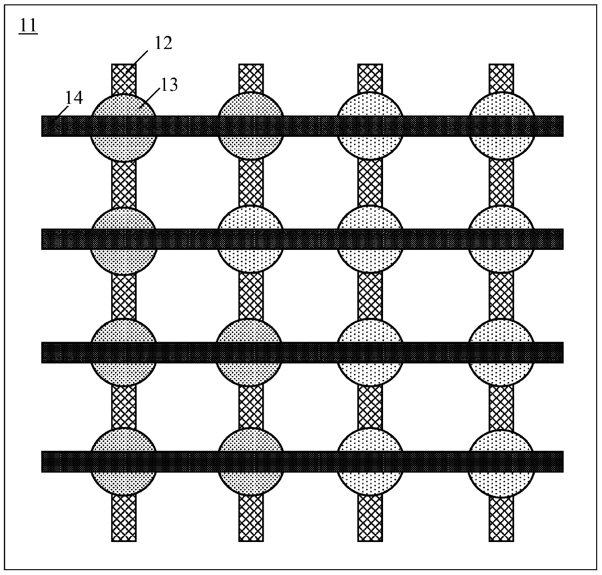
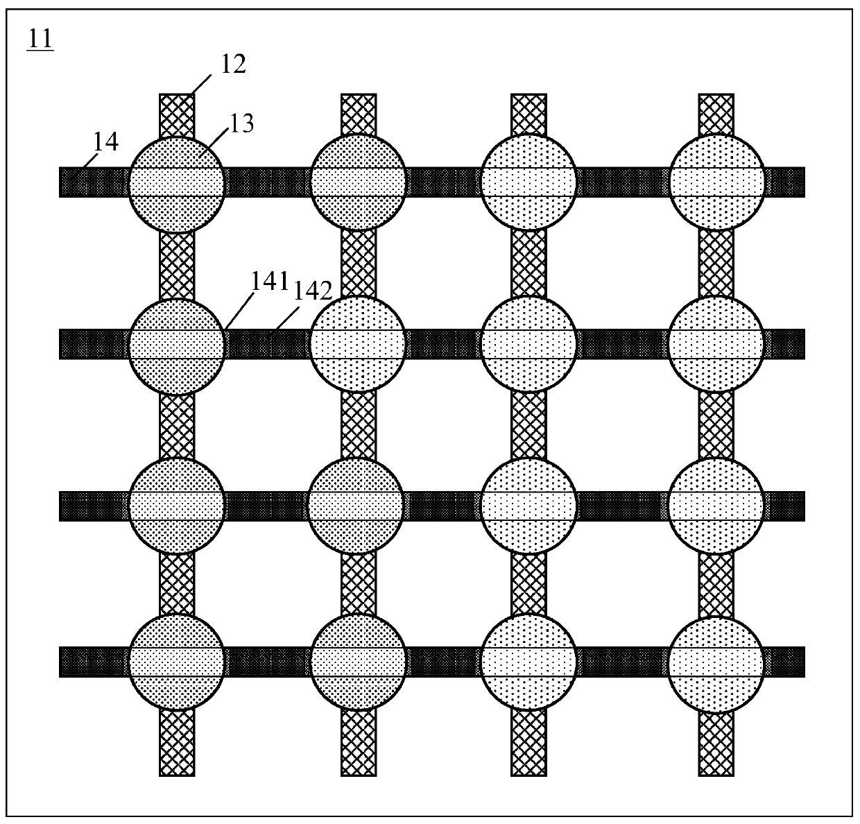
[0034] On the one hand, the embodiments of the present invention provide a fingerprint identification structure, such as figure 1 shown, including:

[0035] Substrate substrate 11;

[0036] A plurality of first touch electrodes 12 and a plurality of second touch electrodes 14 formed on the base substrate 11 (the first touch electrodes 12 and the second touch electrodes 14 may also be referred to as fingerprint recognition electrodes), A first touch electrode 11 and a plurality of second touch electrodes 14 inter...


PUM

PropertyMeasurementUnit
thicknessaaaaaaaaaa

Abstract

The invention provides a fingerprint identification structure and a manufacturing method thereof. The fingerprint recognition structure includes: a base substrate, a plurality of first touch electrodes and a plurality of second touch electrodes formed on the base substrate, and a plurality of first touch electrodes and a plurality of second touch electrodes criss-crossed ; A plurality of light-sensing patterns are correspondingly disposed at positions where the first touch electrodes intersect with the second touch electrodes, and separate the second touch electrodes from the first touch electrodes. In the present invention, the photosensitive pattern between the first touch electrode and the second touch electrode constitutes a photodiode structure. When the light reflected by the finger passes through the light-emitting diode, the light-emitting diode can generate current to increase the signal difference at the valley and ridge position of the fingerprint, so that the fingerprint can be identified more sensitively, thereby reducing the contact between the finger and the first touch electrode, The requirement for the distance between the second touch electrodes enables the subsequently deposited protective layer to be made thicker, so as to increase the structural stability of the device.

Description

technical field [0001] The invention relates to the field of fingerprint identification, in particular to a fingerprint identification structure and a manufacturing method thereof. Background technique [0002] With the popularity of fingerprint identification applications, fingerprint identification technology has been continuously developed. At present, the user's fingerprint can be identified through the display screen. The principle is to set a capacitive fingerprint identification structure on the display substrate. The specific structure is to form multiple lateral electrodes Tx on the display substrate. 1 -Tx n and multiple longitudinal electrodes Rx 1 -Rx n . When entering the fingerprint identification stage, Tx 1 When the drive signal is input (Tx 2 ~Tx n ground handling), Rx 1 to Rx n Receive signals in sequence, then Tx 2 Input drive signal, Rx 1 to Rx n Receive signals in turn... [0003] After the finger is pressed, the valleys or ridges of the fin...

Claims


Application Information

Patent Timeline
Patent Type & Authority Patents(China)
IPC IPC(8): G06K9/00
CPCG06V40/1318G06F3/0446G06V40/1365
Inventor 刘英明吕敬王海生吴俊纬丁小梁许睿赵利军李昌峰贾亚楠郭玉珍秦云科顾品超
Owner BOE TECH GRP CO LTD
Why Eureka
Try Eureka