Straight-plate practical radio frequency MEMS switch
A straight-type, switch technology, applied in the field of radio frequency MEMS, can solve the problems of lower switch yield, difficult process, complex upper electrode structure, etc., to facilitate characteristic impedance matching, avoid ablation and adhesion, and improve yield Effect
- Summary
- Abstract
- Description
- Claims
- Application Information
AI Technical Summary
Problems solved by technology
Method used
Image

Examples
Embodiment Construction
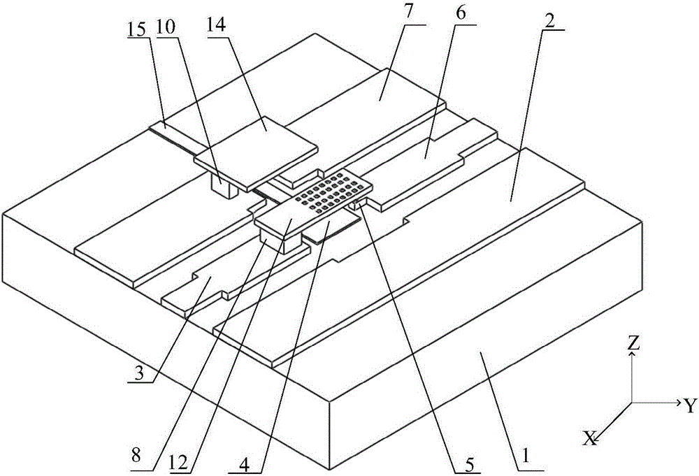
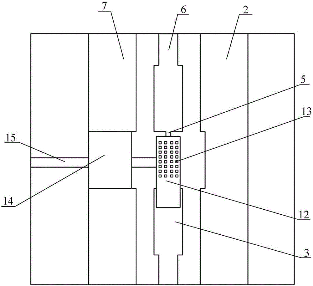
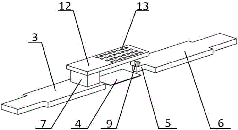
[0039] Embodiments of the present invention are described in detail below, examples of which are shown in the drawings, wherein the same or similar reference numerals designate the same or similar elements or elements having the same or similar functions throughout. The embodiments described below by referring to the figures are exemplary only for explaining the present invention and should not be construed as limiting the present invention.
[0040] In the description of the present invention, it should be understood that the orientations or positional relationships indicated by the terms "center", "upper", "lower", "front", "rear", "left", "right" etc. are based on the attached The orientation or positional relationship shown in the figure is only for the convenience of describing the present invention and simplifying the description, and does not indicate or imply that the referred combination or element must have a specific orientation, be constructed and operated in a spec...
PUM
 Abstract
Description
Claims
Application Information
 - Generate Ideas
- Intellectual Property
- Life Sciences
- Materials
- Tech Scout
- Unparalleled Data Quality
- Higher Quality Content
- 60% Fewer Hallucinations
Browse by: Latest US Patents, China's latest patents, Technical Efficacy Thesaurus, Application Domain, Technology Topic, Popular Technical Reports.
© 2025 PatSnap. All rights reserved.Legal|Privacy policy|Modern Slavery Act Transparency Statement|Sitemap|About US| Contact US: help@patsnap.com