A circuit and memory chip for repairing memory
A memory and circuit technology, applied in the electronic field, can solve problems such as interface incompatibility, and achieve the effect of ensuring compatibility
- Summary
- Abstract
- Description
- Claims
- Application Information
AI Technical Summary
Problems solved by technology
Method used
Image
Examples
Embodiment 1
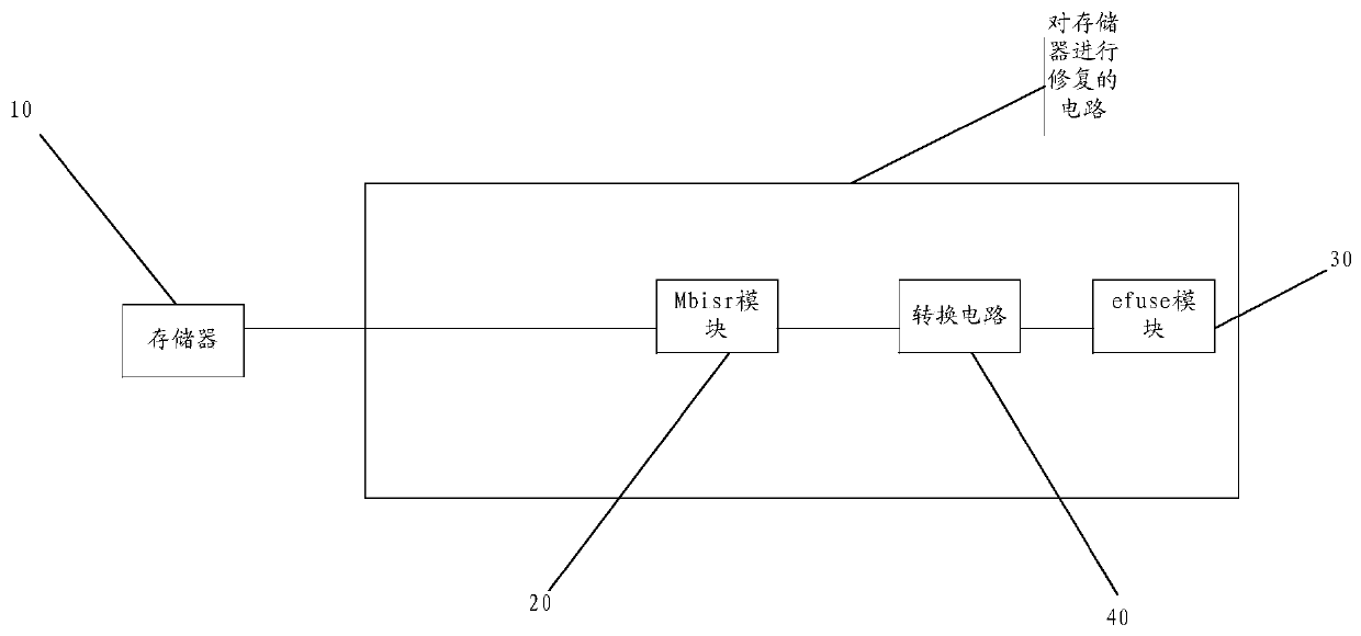
[0058] Please refer to figure 1 , the embodiment of the present application provides a circuit for repairing the memory, including:
[0059] The memory built-in self-repairing Mbisr module 20 is connected with the memory 10, and the Mbisr module 20 is used to determine the failure information when the memory 10 fails;
[0060] An electrically programmable fuse efuse module 30, configured to store the fault information;
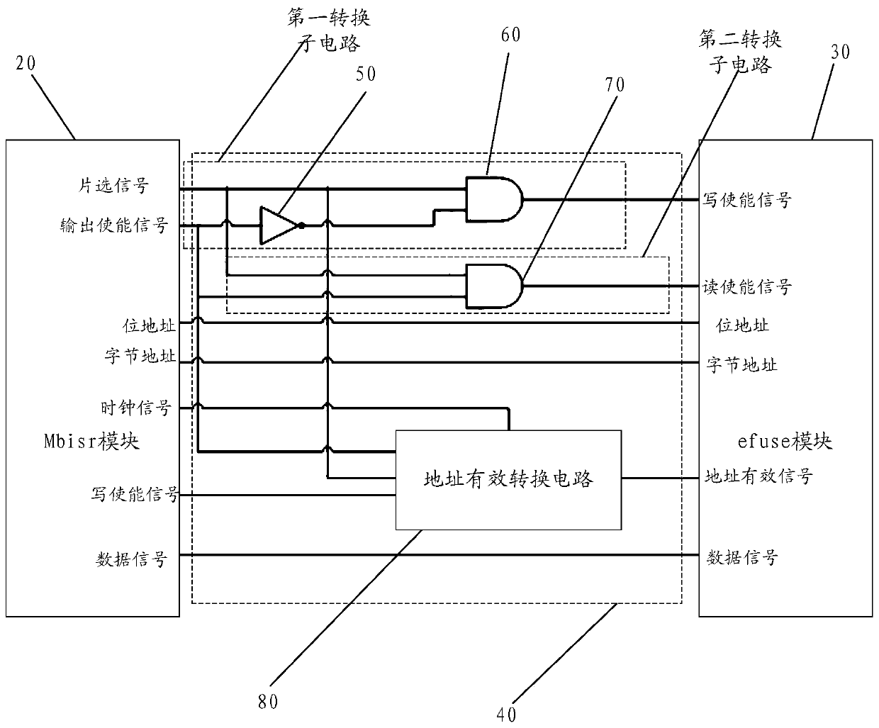
[0061] The conversion circuit 40 is arranged between the Mbisr module 20 and the efuse module 30, and is respectively connected to the interface of the Mbisr module 20 and the interface of the efuse module 30;
[0062] Wherein, conversion circuit 40 is used for when the interface of Mbisr module 20 and the interface of efuse module 30 are different timing interfaces, the read operation signal or write operation signal of Mbisr module 20 to efuse module is converted into can be used by efuse module 30 The signal identified, so that the efuse module 30 can sto...
Embodiment 2
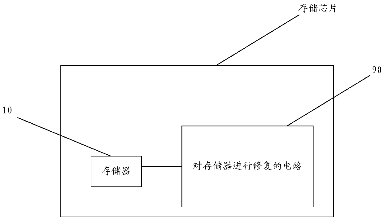
[0077] Please refer to image 3 , based on the same inventive concept as the first embodiment of the present application, the second embodiment of the present application also provides a memory chip, including:
[0078] memory 10;
[0079] Memory built-in self-repair Mbisr module 20, connected with memory 10, Mbisr module 20 is used to determine fault information when memory 10 breaks down;
[0080] The conversion circuit 40 is arranged between the Mbisr module 20 and the efuse module 30, and is connected with the interface of the Mbisr module 20 and the efuse module 30 respectively;
[0081] Wherein, the conversion circuit 40 is used to convert the read operation signal or the write operation signal of the conversion circuit 40 to the efuse module 30 by the conversion circuit 40 to be recognized by the efuse module 30 when the interface of the conversion circuit 40 and the interface of the efuse module 30 are different timing interfaces. signal, so that the efuse module 30 ...
PUM
 Abstract
Description
Claims
Application Information


