Circuit of repairing memory and storage chip

A memory and circuit technology, applied in the electronic field, can solve problems such as interface incompatibility, and achieve the effect of ensuring compatibility

Active Publication Date: 2017-12-08
北京东土军悦科技有限公司 +1
View PDF3 Cites 0 Cited by
  • Summary
  • Abstract
  • Description
  • Claims
  • Application Information

AI Technical Summary

Problems solved by technology

[0007] The embodiment of the present invention provides a circuit and a memory chip for repairing the memory, which are used to solve the technical problem of the interface incompatibility between the Mbisr module and the efuse module that have different timing interfaces in the memory chip in the prior art, and ensure the memory Compatibility between the Mbisr module interface and the efuse module interface of different timing interfaces in the chip

Method used


Image

  • Circuit of repairing memory and storage chip
  • Circuit of repairing memory and storage chip
  • Circuit of repairing memory and storage chip

Examples


Embodiment 1

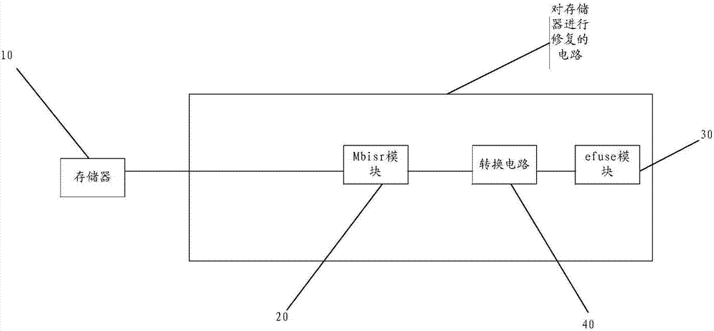
[0058] Please refer to figure 1 , the embodiment of the present application provides a circuit for repairing the memory, including:

[0059] The memory built-in self-repairing Mbisr module 20 is connected with the memory 10, and the Mbisr module 20 is used to determine the failure information when the memory 10 fails;

[0060] An electrically programmable fuse efuse module 30, configured to store the fault information;

[0061] The conversion circuit 40 is arranged between the Mbisr module 20 and the efuse module 30, and is respectively connected to the interface of the Mbisr module 20 and the interface of the efuse module 30;

[0062] Wherein, conversion circuit 40 is used for when the interface of Mbisr module 20 and the interface of efuse module 30 are different timing interfaces, the read operation signal or write operation signal of Mbisr module 20 to efuse module is converted into can be used by efuse module 30 The signal identified, so that the efuse module 30 can sto...

Embodiment 2

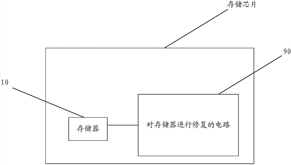
[0077] Please refer to image 3 , based on the same inventive concept as the first embodiment of the present application, the second embodiment of the present application also provides a memory chip, including:

[0078] memory 10;

[0079] Memory built-in self-repair Mbisr module 20, connected with memory 10, Mbisr module 20 is used to determine fault information when memory 10 breaks down;

[0080] The conversion circuit 40 is arranged between the Mbisr module 20 and the efuse module 30, and is connected with the interface of the Mbisr module 20 and the efuse module 30 respectively;

[0081] Wherein, the conversion circuit 40 is used to convert the read operation signal or the write operation signal of the conversion circuit 40 to the efuse module 30 by the conversion circuit 40 to be recognized by the efuse module 30 when the interface of the conversion circuit 40 and the interface of the efuse module 30 are different timing interfaces. signal, so that the efuse module 30 ...


PUM


Abstract

The invention provides a circuit of repairing a memory and a storage chip. The circuit of repairing the memory includes: a memory built-in self-repair (Mbisr) module, which is connected with the memory and used for determining fault information when a fault of the memory occurs; an electrically programmable fuse (efuse) module, which is used for storing the fault information; and a conversion circuit, which is disposed between the Mbisr module and the efuse module and respectively connected with an interface of the Mbisr module and an interface of the efuse module. The conversion circuit is used for converting a reading operation signal or a writing operation signal of the Mbisr module on the efuse module into a signal, which can be identified by the efuse module, when the interface of the Mbisr module and the interface of the efuse module are different time sequence interfaces. Signals which can be identified by the efuse module include a writing enabling signal of the efuse module, a reading enabling signal of the efuse module, an address validity signal and a data input signal.

Description

technical field [0001] The invention relates to the field of electronic technology, in particular to a circuit and a memory chip for repairing a memory. Background technique [0002] The minimum process precision of existing chip production is getting higher and higher, and the demand for memory repair functions is also increasing. [0003] The memory built-in self-repair module (Memory built-in self-repair, Mbisr module) is a module built in on the chip for repairing the memory, and the Mbisr module is outside the memory. During the memory development process, the Mbisr module tests the memory, and if the memory is found to be defective, the fault information is stored in the efuse module (electrically programmable fuse, electrically programmable fuse module) for fault repair. [0004] Specifically, the technology of using the efuse module to repair the memory is mainly based on the characteristics of polysilicon fuses. Taking advantage of the small initial resistance of ...

Claims


Application Information

Patent Timeline
Patent Type & Authority Applications(China)
IPC IPC(8): G11C17/16G11C29/44
CPCG11C17/16G11C29/44
Inventor 李智韬
Owner 北京东土军悦科技有限公司
Why Eureka
Try Eureka