
Detection circuit and method of storage elements in FPGA (Field Programmable Gate Array) chip

A technology of storage elements and detection circuits, applied in static memory, instruments, etc., can solve the problems that Virtex-7 is not applicable, there is no Virtex-7 trigger and latch positioning, etc.

Inactive Publication Date: 2017-12-08
CHINA ACADEMY OF SPACE TECHNOLOGY
View PDF11 Cites 1 Cited by
  • Summary
  • Abstract
  • Description
  • Claims
  • Application Information

AI Technical Summary

Problems solved by technology

[0008] The existing detection methods for storage components are all detection methods for Xilinx’s early Virtex, Virtex-II and other types of storage components. Since the structure of the CLB SLICE of the Virtex-7 series has been greatly improved,

Method used


Image

  • Detection circuit and method of storage elements in FPGA (Field Programmable Gate Array) chip
  • Detection circuit and method of storage elements in FPGA (Field Programmable Gate Array) chip
  • Detection circuit and method of storage elements in FPGA (Field Programmable Gate Array) chip

Examples


Embodiment Construction

[0055] The specific implementation manners of the present invention will be further described in detail below in conjunction with the accompanying drawings and embodiments. The following examples are used to illustrate the present invention, but are not intended to limit the scope of the present invention.

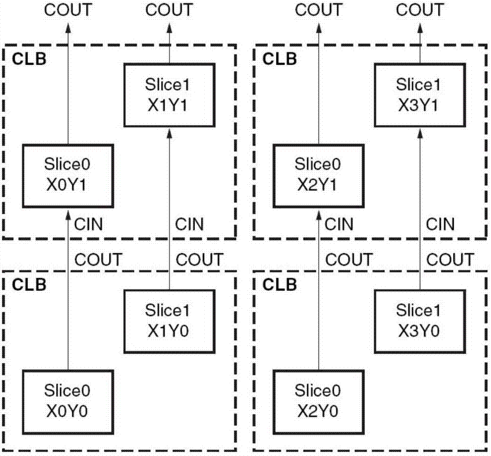
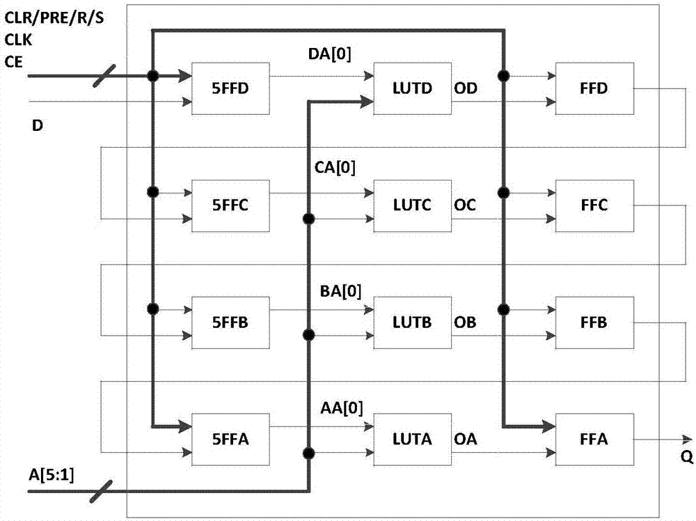
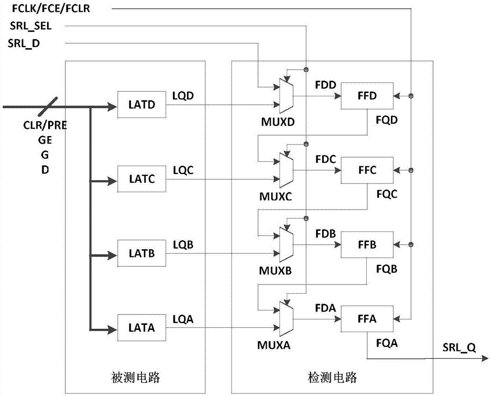
[0056] The detection circuit of the present invention comprises an FDCE detection circuit, an FDPE detection circuit, an FDRE detection circuit, an FDSE detection circuit, an LDCE detection circuit and an LDPE detection circuit, wherein the FDCE detection circuit, the FDPE detection circuit, the FDRE detection circuit, and the FDSE detection circuit are basically the same, and the difference The only difference lies in the definition of a control pin of the storage element circuit primitive used (respectively corresponding to asynchronous reset CLR, asynchronous set PRE, synchronous reset R, synchronous set S), such as figure 2 As shown, collectively referred to as "trigg...


PUM


Abstract

The invention provides a detection circuit and method of storage elements in an FPGA (Field Programmable Gate Array) chip. The circuit comprises slices, wherein each slice comprises a plurality of channels and each channel comprises a first element, a lookup table and a second element which are connected in sequence; each second element is connected with the first element of the next channel. When the elements receive a first clock signal, a detection signal is received and stored; when the elements receive a second clock signal, a reference signal is received and stored and a result is output. Or the circuit comprises a detected circuit and a detection circuit in two slices of a configurable logic block; the detected circuit is provided with a plurality of third elements to be detected and the detection circuit is provided with a plurality of channels for connecting the lookup tables and fourth elements; each fourth element is connected with input of the lookup table of the next channel; each third element is connected with the other input of the lookup table. The third elements are used for receiving and storing the detection signal and the lookup tables are used for receiving the reference and detection signals and outputting the reference and detection signals to the fourth elements; when the fourth elements receive a fourth clock signal, the detection signals are received and stored; when the fourth elements receive a fifth clock signal, the reference signal is received and stored and the result is output. The elements are storage elements.

Description

technical field [0001] The invention relates to the field of integrated circuit chip testing, in particular to a detection circuit and a detection method of a storage element in an SRAM FPGA chip. Background technique [0002] FPGA (Field-Programmable Gate Array), that is, field programmable gate array, is a product of further development on the basis of programmable devices such as PAL, GAL, and CPLD. [0003] Xilinx 7 series FPGA includes Artix-7, Kentix-7 and Virtex-7 three subclasses. The configurable logic block (CLB) structure of the three types of devices is the same, such as figure 1 shown. Each CLB consists of 2 slices (SLICE), and each slice has a unique physical location number (such as X0Y0, X2Y1). [0004] Storage Element (Storage Element) is a functional module in FPGA SLICE that implements programmable sequential logic, and is a key unit for synchronous design, establishment of pipeline structure, and improvement of FPGA internal logic operation speed. The ...

Claims


Application Information

Patent Timeline
IPC IPC(8): G11C29/56
CPCG11C29/56
Inventor 王贺王熙庆汪悦张红旗宁永成张大宇张松蒋承志丛山姜琳
Owner CHINA ACADEMY OF SPACE TECHNOLOGY
Learn More