Gigabit switch supporting improved layer 3 switching

a gigabit switch and layer 3 technology, applied in data switching networks, instruments, high-level techniques, etc., can solve the problems of increasing design requirements, increasing design complexity, and relatively slow conventional dynamic random access memory (dram) speed, and achieve the effect of improving layer 3 switching

Active Publication Date: 2006-03-07
AVAGO TECH INT SALES PTE LTD
View PDF63 Cites 134 Cited by
  • Summary
  • Abstract
  • Description
  • Claims
  • Application Information

AI Technical Summary

Benefits of technology

[0010]More specifically, the present invention is directed to a switch with improved layer 3 switching. With the layer 3 forwarding being performed in hardware, the routing can be performed at line speed. Having the switch perform the layer 3 switching also eliminate

Problems solved by technology

As speed has increased, design constraints and design requirements have become more and more complex with respect to following appropriate design and protocol rules and providing a low cost, commercially viable solution.
For example, high speed switching requires high speed memory to provide appropriate buffering of packet data; conventional Dynamic Random Access Memory (DRAM) is relatively slow, and requires hardware-driven refresh.
The speed of DRAMs, therefore, as buffer memory in network switching, results in valuable time being lost, and it becomes

Method used


Image

  • Gigabit switch supporting improved layer 3 switching
  • Gigabit switch supporting improved layer 3 switching
  • Gigabit switch supporting improved layer 3 switching

Examples


case b

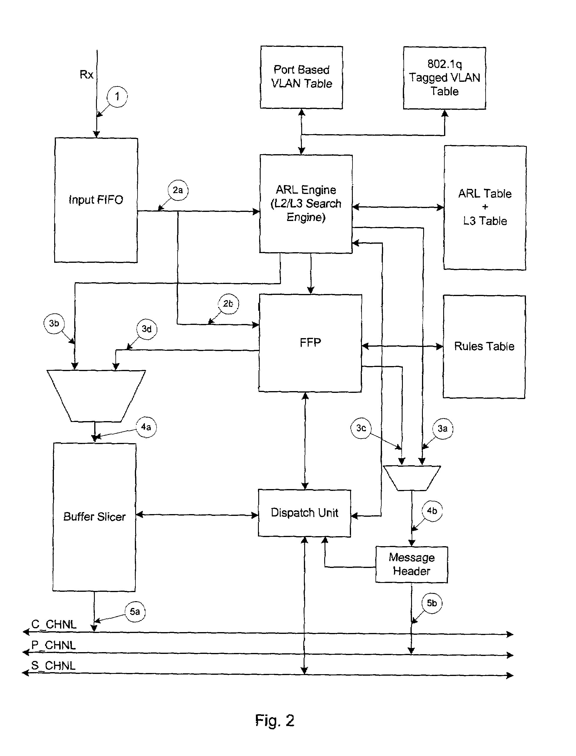
[0247]The following rules are applied to conflicts:[0248]Rule 1.—When there is a conflict of actions across the filters, then the action associated with the highest filter is carried out.[0249]Rule 2.—When there is conflict of actions within the same filter, the following priorities hold. Six cases are possible.[0250]CASE A: Conflict in 802.1p priority, then change 802.1p priority—Action 0 (Medium) and change TOS to 802.1p—Action 8 (Low)[0251] Conflict in COS Queue, then change Priority 802.1p—Action 0 (Medium), re-map to new COS—Action 1 (Low), and change TOS to 802.1p—Action 8 (Low Low)[0252]CASE C: Conflict in TOS / DiffServ Field, then change TOS P field—Action 2 (Medium), change COS to TOS_P—Action 9 (Low); and DiffServ—Action 10 (High)[0253]CASE D: Action bits 5 and 11, select Output port—Action 5 (Low) and select Output port, Output Module Id—Action 11 (High).[0254]CASE E: Action bits within the same IMASK, then select FFP Drop (Low) and select FFP No-Drop (High)[0255]CASE F: A...


PUM


Abstract

A network switch for network communications is disclosed. The switch includes a first data port interface, supporting at least one data port transmitting and receiving data at a first data rate and a second data port interface supporting a at least one data port transmitting and receiving data at a second data rate. The switch also has a CPU interface configured to communicate with a CPU and a memory management unit for communicating data from at least one of the first and second data port interfaces and a memory. It also has a communication channel for communicating data and messaging information between the first and second data port interfaces and the memory management unit and a plurality of semiconductor-implemented lookup tables including an address resolution lookup table, a layer three IP lookup table and VLAN tables. One of the first and second data port interfaces is configured to determine whether an incoming data packet is a unicast packet, a multicast packet or an IP multicast packet; and the address resolution lookup and layer three IP lookup tables are searched to find an egress port for the incoming data packet.

Description

REFERENCE TO RELATED APPLICATIONS[0001]This application claims priority of U.S. Provisional Patent Application Serial No. 60 / 210,510, filed on Jun. 9, 2000 and United States Provisional Patent Application Ser. No. 60 / 270,158, filed on Feb. 22, 2001. The contents of the provisional applications are hereby incorporated by reference.BACKGROUND OF THE INVENTION[0002]1. Field of the Invention[0003]The invention relates to an apparatus for high performance switching in local area communications networks such as token ring, ATM, ethernet, fast ethernet, and gigabit ethernet environments, generally known as LANs. In particular, the invention relates to a new switching architecture in an integrated, modular, single chip solution, which can be implemented on a semiconductor substrate such as a silicon chip.[0004]2. Description of the Related Art[0005]As computer performance has increased in recent years, the demands on computer networks has significantly increased; faster computer processors ...

Claims


Application Information

Patent Timeline
IPC IPC(8): H04L12/56F01D9/04G06F15/173H04J3/24H04L12/18H04L12/28H04L12/46
CPCH04L12/462H04L45/16H04L45/245H04L45/52H04L45/742H04L47/10H04L47/2458H04L47/266H04L47/29H04L47/32H04L49/109H04L49/15H04L49/351H04L45/00H04L69/22H04L49/102H04L49/3009H04L49/3018H04L49/3036H04L49/352H04L49/354H04L49/506H04L49/508H04L49/602Y02B60/33Y02D30/50
Inventor AMBE, SHEKHARKALKUNTE, MOHAN
Owner AVAGO TECH INT SALES PTE LTD
Why Eureka
Try Eureka