Liquid crystal panel and manufacturing method thereof and display device

A technology of liquid crystal panel and manufacturing method, which is applied in nonlinear optics, instrumentation, optics, etc., and can solve the problems affecting narrow borders and the impossibility of borderless display

Active Publication Date: 2017-12-22
TCL CHINA STAR OPTOELECTRONICS TECH CO LTD
View PDF7 Cites 26 Cited by
  • Summary
  • Abstract
  • Description
  • Claims
  • Application Information

AI Technical Summary

Problems solved by technology

There is even a "frameless" panel concept, that is, to remove the outer frame that blocks the non-display area of ​​the panel to achieve a borderless display. However, since the bonding end on the TFT substrate side is longer than the CF substrate, a special outer frame needs to be reserved to cover the panel. The connection lines in the binding area affect the narrow border, and the borderless display cannot be realized

Method used


Image

  • Liquid crystal panel and manufacturing method thereof and display device
  • Liquid crystal panel and manufacturing method thereof and display device
  • Liquid crystal panel and manufacturing method thereof and display device

Examples


Embodiment Construction

[0030] In order to make the object, technical solution and advantages of the present invention more clear, the present invention will be further described in detail below in conjunction with the accompanying drawings and embodiments. It should be understood that the specific embodiments described here are only used to explain the present invention, not to limit the present invention.

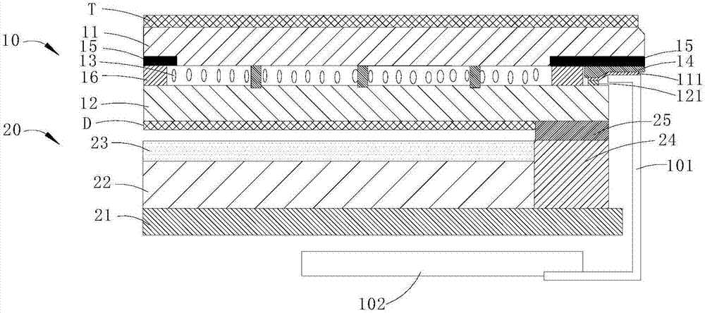
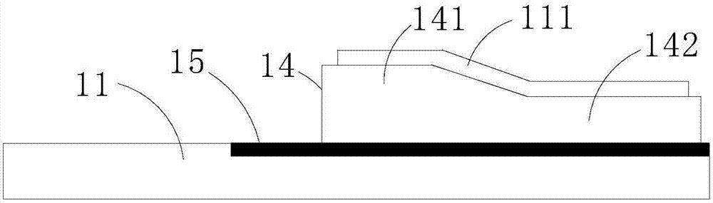
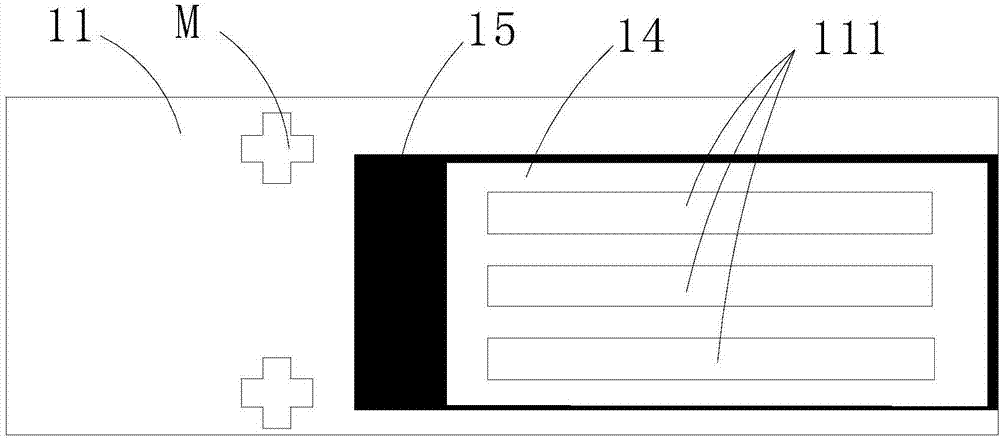
[0031] refer to figure 1 , the display device of the embodiment of the present invention includes a liquid crystal panel 10 and a backlight module 20, the liquid crystal panel 10 includes a color filter substrate 11, an array substrate 12, and a liquid crystal 13 filled between the color filter substrate 11 and the array substrate 12, the backlight module 10 is arranged on the side where the array substrate 12 is located, that is, the light emitted by the backlight module 10 enters the liquid crystal panel 10 from the array substrate 12 side, and is emitted from the color filter substrate 11 sid...


PUM


Abstract

The invention discloses a liquid crystal panel. The liquid crystal panel comprises a color film substrate, an array substrate, liquid crystal between the color film substrate and the array substrate, a photo spacer on the color film substrate, a crystal covering thin film and a circuit board, wherein a conversion terminal set which is led from a signal wire is arranged on the surface of the array substrate, a conducting electrode is arranged on the end surface of the photo spacer, and the photo space abuts one end of the conducting electrode against the conversion terminal set; the other end of the conducting electrode is arranged on a non-display area of the liquid crystal panel and is bound with the crystal covering thin film, and the circuit board is arranged on the side where the array substrate locates. The invention further discloses a manufacturing method of the liquid crystal panel and a display device. The conversion terminal set is formed and led from the signal wire on the surface of the array substrate, the photo spacer is manufactured on the color film substrate side, the photo spacer presses the conducting electrode onto the conversion terminal set, and the conversion terminal set and the crystal covering thin film are bound, accordingly the situation is avoided that the array substrate side extends out of a long binding zone, and the manufacturing method is beneficial for achievement of a super-narrow frame or no frame.

Description

technical field [0001] The invention relates to the technical field of liquid crystal display, in particular to a liquid crystal panel, a manufacturing method thereof, and a display device. Background technique [0002] Chip On Film (COF), which is to fix the chip (IC) on the grain soft film of the flexible circuit board (FPC), is used in many display panels such as LCD, OLED, etc. This packaging technology chip. This kind of chip is mostly used as the source driver (Source Driver) and gate driver (GateDriver) of the display driver. In the drive circuit, one end of the COF is connected to the printed circuit board (PCB), which is responsible for receiving the data signal transmitted from the printed circuit board, and the other end of the COF is connected to the display panel (Panel), which is used to transmit the data signal output by the IC to the on the display panel to drive the display panel for display. [0003] Specifically, the connection of the COF with the print...

Claims


Application Information

Patent Timeline
Patent Type & Authority Applications(China)
IPC IPC(8): G02F1/1345G02F1/1339G02F1/1333
CPCG02F1/1333G02F1/13394G02F1/13452
Inventor 张伟基
Owner TCL CHINA STAR OPTOELECTRONICS TECH CO LTD
Why Eureka
Try Eureka