Shift Register
A technology of shift register and potential, which is applied in static memory, digital memory information, instruments, etc., and can solve problems such as misoperation of shift registers
- Summary
- Abstract
- Description
- Claims
- Application Information
AI Technical Summary
Problems solved by technology
Method used
Image

Examples
no. 1 approach
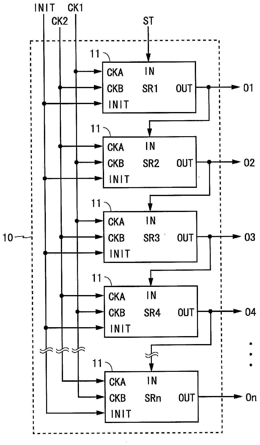
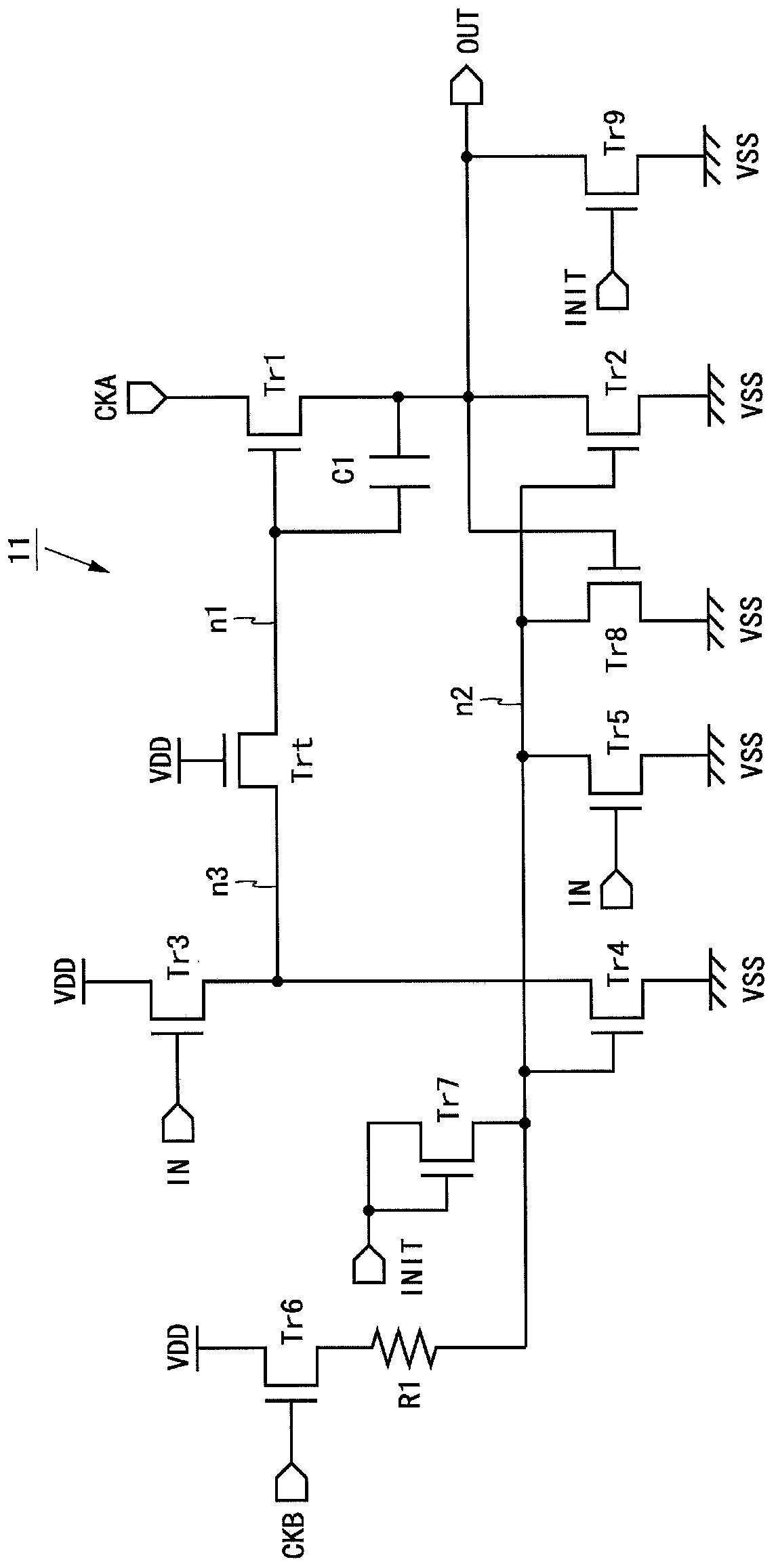
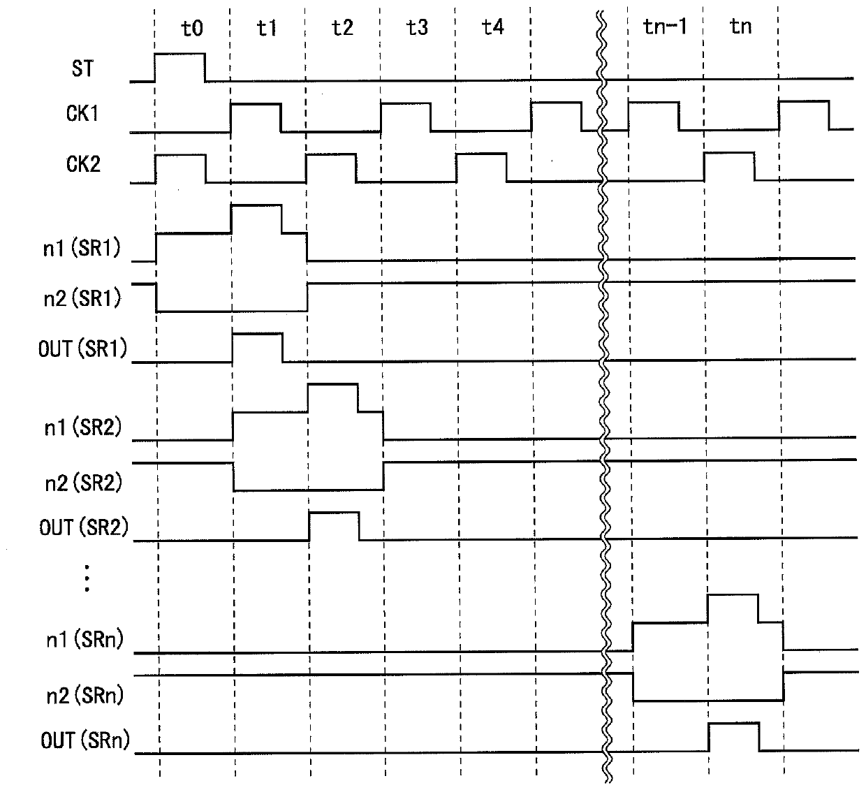
[0111]Hereinafter, a shift register according to an embodiment of the present invention will be described with reference to the drawings. In the following description, when the conduction terminal of a transistor may be a source terminal or a drain terminal, the conduction terminal of one is always referred to as a source terminal, and the conduction terminal of the other is always referred to as a source terminal. drain terminal. In addition, a signal input or output via a certain terminal is called by the same name as the terminal (for example, a signal input via the clock terminal CKA is called a clock signal CKA). In addition, when applied to the gate terminal, the potential that turns on the transistor is called on-potential, and the potential that turns off the transistor is called off-potential. For example, for an N-channel transistor, the high-level potential is the on-potential, and the low-level potential is the off-potential. In addition, the threshold voltage of...
no. 2 approach
[0137] Figure 4 It is a block diagram showing the configuration of the shift register according to the second embodiment of the present invention. Figure 4 The shown shift register 20 is configured by adding a function of switching the scanning direction (shift direction) to the shift register 10 according to the first embodiment. The shift register 20 includes n unit circuits 11 and n selection circuits 22 . The n unit circuits 11 and the n selection circuits 22 are provided in one-to-one correspondence. Hereinafter, the selection circuit corresponding to the unit circuit Sri of the i-th stage is referred to as the selection circuit SELi of the i-th stage. The selection circuit 22 has input terminals IN1, IN2, control terminals UD, UDB, and an output terminal Z. The shift register 20 is externally supplied with a start signal ST, two-phase clock signals CK1 and CK2 , an initialization signal INIT, and control signals UD and UDB. The control signal UDB is a negative (Neg...
no. 3 approach
[0144] Image 6 It is a block diagram showing the configuration of the shift register according to the third embodiment of the present invention. Image 6 The shift register 30 shown has a configuration in which n unit circuits 31 are connected in multiple stages. The unit circuit 31 has an input terminal IN, clock signals CKA, CKB, an initialization terminal INIT, all-on control terminals AON, AONB, and an output terminal OUT. The shift register 30 is externally supplied with a start signal ST, two-phase clock signals CK1, CK2, an initialization signal INIT, an all-on control signal AON, and a negation signal AONB of the all-on control signal (hereinafter referred to as the negation signal AONB for short). ).
[0145] The start signal ST is supplied to the input terminal IN of the primary unit circuit 31 . The clock signals CK1 and CK2 and the initialization signal INIT are supplied to the n unit circuits 31 in the same manner as the shift register 10 according to the firs...
PUM
 Abstract
Description
Claims
Application Information
 - R&D Engineer
- R&D Manager
- IP Professional
- Industry Leading Data Capabilities
- Powerful AI technology
- Patent DNA Extraction
Browse by: Latest US Patents, China's latest patents, Technical Efficacy Thesaurus, Application Domain, Technology Topic.
© 2024 PatSnap. All rights reserved.Legal|Privacy policy|Modern Slavery Act Transparency Statement|Sitemap