A method of manufacturing a pcb

A production method and solder mask technology, applied in the direction of electrical connection of printed components, printed circuit components, printed circuits, etc., can solve problems such as failure, pin corrosion, etc., and achieve the effect of preventing the residue of potion or water vapor

Active Publication Date: 2019-11-05
DONGGUAN SHENGYI ELECTRONICS
View PDF6 Cites 0 Cited by
  • Summary
  • Abstract
  • Description
  • Claims
  • Application Information

AI Technical Summary

Problems solved by technology

[0003] However, the above solution has the following problems: After the welding is completed, if there is liquid medicine residue or water vapor in the hole, long-term use will cause corrosion of the pins and bring the risk of failure

Method used


Image

  • A method of manufacturing a pcb
  • A method of manufacturing a pcb
  • A method of manufacturing a pcb

Examples


Embodiment 1

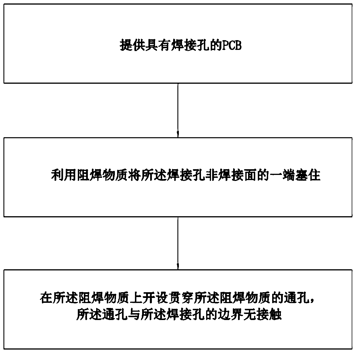
[0062] Such as figure 1 , 3 , 6 and 7, the present embodiment provides a method for manufacturing a PCB, comprising the following steps:

[0063] Step 1, providing PCB1 with soldering holes 11;

[0064] Step 2, using a solder resist material to plug one end of the non-welding surface of the welding hole 11;

[0065] Step 3, opening a through hole penetrating through the solder resist material on the solder resist material, and the through hole has no contact with the boundary of the solder hole 11 .

[0066] Specifically, after the welding hole 11 is plugged with a solder resist material, a through hole through the solder resist material is opened, and at the same time, the through hole does not overlap with the boundary of the welding hole 11, and the solder resist material completely surrounds the inner wall of the solder hole 11 to form a solder resist Ring 4, so when welding components or connectors on PCB1, the solder is blocked by the solder resist ring 4 during the c...

Embodiment 2

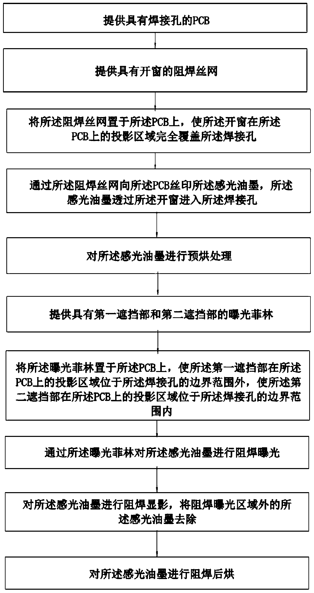
[0069] Such as Figure 2-7 As shown, the present embodiment provides a method for manufacturing a PCB, comprising the following steps:

[0070] Step 1, providing a PCB 1 with soldering holes 11 .

[0071] The aforementioned PCB1 with soldering holes 11 can be the PCB1 in any state before the PCB1 is finished. The welding holes 11 can also be equivalently replaced with welding slots.

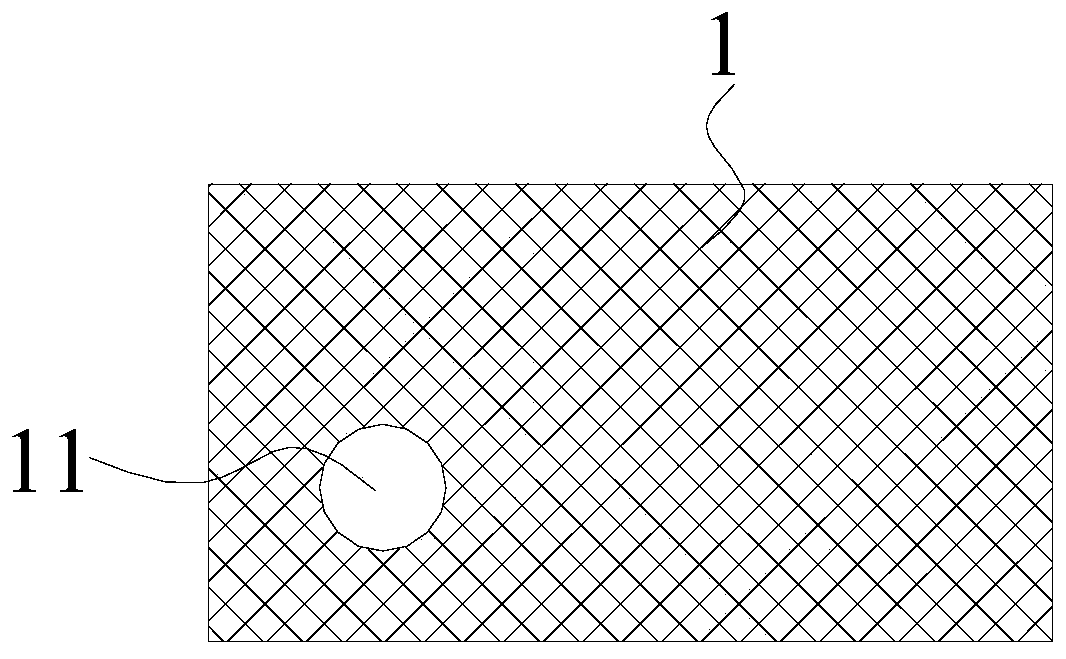
[0072] Step 2, providing the solder resist wire mesh 3 with windows 31 .

[0073] The material of the solder resist screen 3 is metal or polymer fiber, but not limited to the above materials.

[0074] Step 3, placing the solder resist screen 3 on the PCB 1 so that the projected area of ​​the window 31 on the PCB 1 completely covers the solder hole 11 .

[0075] Step 4: Screen printing the photosensitive ink on the PCB 1 through the solder resist screen 3 , and the photosensitive ink enters the soldering hole 11 through the window 31 .

[0076] The projected area of ​​the window 31 on the PCB...

Embodiment 3

[0097] Such as Figure 6-7 As shown, a PCB, the PCB1 is provided with a welding hole 11, and the inner wall of the welding hole 11 is provided with a solder resist ring 4, and the material of the solder resist ring 4 is photosensitive ink.

[0098] The solder resist ring 4 surrounds the inner wall of the solder hole 11 , but does not completely block the solder hole 11 (that is, both ends of the solder hole 11 still pass through). When soldering components or connectors on the PCB1, the solder resist ring 4 can prevent the solder from easily climbing up to the other side of the board along the copper surface on the inner wall of the solder hole 11, and at the same time, because the solder resist ring 4 does not completely block the solder hole 11, It also prevents the solder from having liquid medicine or water vapor remaining in the soldering hole 11.

[0099] Further, the height of the solder resist ring 4 is greater than or equal to 0.3 mm.

[0100] The height of the solder...


PUM


Abstract

The invention discloses a manufacturing method of a PCB (Printed Circuit Board), and relates to the field of PCB manufacturing. The manufacturing method comprises the steps of providing a PCB with a welding hole; plugging the end of a non-welding surface of the welding hole by using a solder resisting substance; and forming a through hole, which penetrates through the solder resisting substance, on the solder resisting substance, wherein the through hole is not contacted with the boundary of the welding hole. According to the method, a solder resisting ring formed by the solder resisting substance is formed in the welding hole, and the solder resisting ring on the PCB manufactured according to the method can avoid the welding flux from climbing to the board surface at the other side alonga copper surface on the inner wall of the welding hole. Meanwhile, the solder resisting ring does not completely block the welding hole, so that the welding flux is also prevented from having liquid medicine or water vapor residue in the welding hole, pins of components are not corroded after long-time use, and the failure risk is low.

Description

technical field [0001] The invention relates to the technical field of PCB manufacturing, in particular to a method for manufacturing a PCB. Background technique [0002] When the PCB is soldering components and connectors, the solder tends to climb up from the copper surface on the inner wall of the welding hole to the other side of the board surface, posing various hidden dangers to the circuit. The solution in the prior art uses a solder mask half-plug process to seal the non-welding surface. [0003] However, the above solution has the following problems: after the welding is completed, if there is liquid medicine residue or water vapor in the hole, long-term use will cause corrosion of the pins and bring the risk of failure. Contents of the invention [0004] An object of the present invention is to provide a PCB manufacturing method, which can form a solder resist ring made of photosensitive ink in the solder hole, and the solder resist ring can prevent the solder f...

Claims


Application Information

Patent Timeline
Patent Type & Authority Patents(China)
IPC IPC(8): H05K1/11H05K3/28
CPCH05K1/116H05K3/28H05K2201/09581
Inventor 万里鹏纪成光刘梦茹金侠
Owner DONGGUAN SHENGYI ELECTRONICS
Why Eureka
Try Eureka