Brightness compensation device and method and storage unit

A brightness compensation and memory technology, applied in the field of liquid crystal display, can solve the problems of limited internal space, uncertainty of display effect, large storage capacity, etc., to achieve the effect of improving uniformity, improving display effect and saving storage space

Active Publication Date: 2018-03-13
WUHAN CHINA STAR OPTOELECTRONICS SEMICON DISPLAY TECH CO LTD
View PDF6 Cites 36 Cited by
  • Summary
  • Abstract
  • Description
  • Claims
  • Application Information

AI Technical Summary

Problems solved by technology

In this method, each pixel needs to pre-store the brightness compensation factor, which requires a large storage capacity. However, due to the limited internal space of the DRIVER IC, arranging a large-capacity storage area will face great difficulties in terms of design difficulty and cost.
Moreover, the GAMMA curve of each pixel is fitted based on several gra

Method used


Image

  • Brightness compensation device and method and storage unit
  • Brightness compensation device and method and storage unit
  • Brightness compensation device and method and storage unit

Examples


Embodiment 1

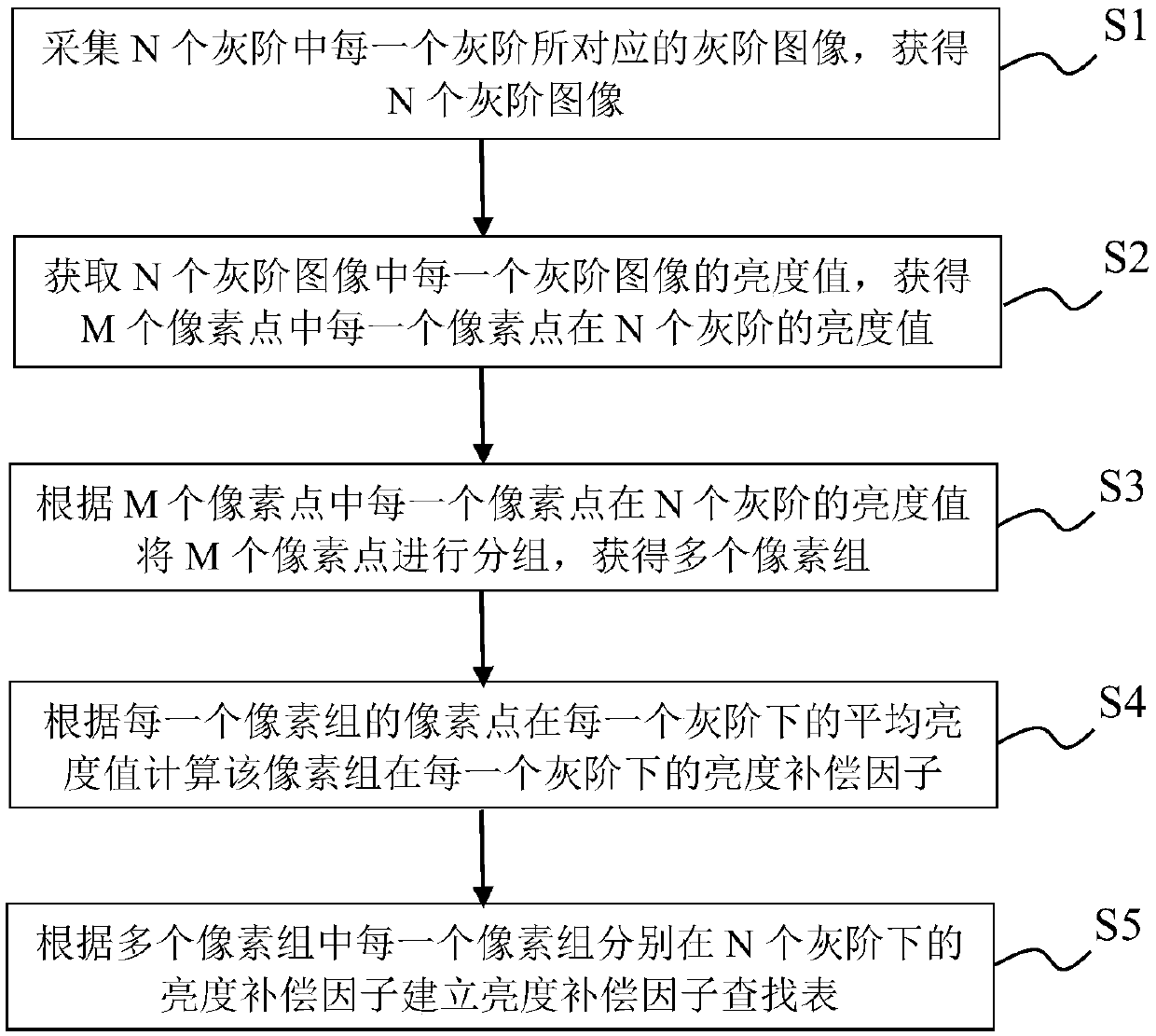
[0044] refer to figure 1 The method for brightness compensation provided in this embodiment includes the steps of:

[0045] S1. Collect the gray-scale images corresponding to each of the N gray-scales to obtain N gray-scale images;

[0046] S2. Obtain the luminance values ​​of M pixels in each of the N gray-scale images, and obtain the luminance values ​​of each of the M pixels in N gray-scales;

[0047] S3. Group the M pixels according to the brightness value of each of the M pixels in N gray scales to obtain multiple pixel groups;

[0048] S4. Calculate the brightness compensation factor of the pixel group at each gray scale according to the average brightness value of the pixel points of each pixel group in each pixel group at each gray scale, and obtain each pixel in the multiple pixel groups The brightness compensation factors of each group under N gray scales;

[0049] S5. Establish a brightness compensation factor lookup table according to the brightness compensation...

Embodiment 2

[0068] The difference between this embodiment and Embodiment 1 lies in the adopted grouping method and the method of establishing the brightness compensation factor lookup table.

[0069] Step S3 in this embodiment includes:

[0070] S31. Calculate the difference between the luminance values ​​of any two pixels among the M pixels in each gray scale. As an example, the luminance values ​​of 5 pixels in 3 gray scales are respectively (x 11 ,y 12 ,z 13 ), (x 21 ,y 22 ,z 23 ), (x 31 ,y 32 ,z 33 ), (x 41 ,y 42 ,z 43 ), (x 51 ,y 52 ,z 53 ), calculate the difference between the brightness values ​​of the first pixel point and the second, third, fourth, and fifth pixel points under the three gray scales as x 11 -x 21 ,y 12 -y 22 ,z 13 -z 23 , x 11 -x 31 ,y 12 -y 32 ,z 13 -z 33 , x 11 -x 41 ,y 12 -y 42 ,z 13 -z 43 , x 11 -x 51 ,y 12 -y 52 ,z 13 -z 53 .

[0071] S32. If the brightness difference between two pixels in each gray scale is smaller than ...


PUM


Abstract

The invention provides a brightness compensation device and method, and a storage unit. The method comprises the steps: acquiring a grayscale image corresponding to each of N gray levels; obtaining the brightness values of M pixels of each of N grayscale images; grouping M pixels according to the brightness values of each of M pixels at N gray levels, and obtaining a plurality of pixel groups; calculating the brightness compensation factor of each pixel group at each gray level according to the mean brightness value of pixels of each of the pixel groups at each gray level, an obtaining the brightness compensation factors of each of pixel groups at N gray levels; building a brightness compensation factor look-up table according to the brightness compensation factors of each of pixel groupsat N gray levels. The method provided by the invention improves the uniformity of the brightness of a display, improves the display effect of the display, and saves the storage space of the display.

Description

technical field [0001] The invention relates to the technical field of liquid crystal display, in particular to a brightness compensation device and method, and a memory. Background technique [0002] Due to the manufacturing process of OLED products, the consistency of each pixel is poor. OLED products without any treatment will have more serious brightness unevenness (MURA). Therefore, before the OLED products leave the factory, it is necessary to perform brightness compensation (DEMURA) on each OLED product. [0003] At present, DEMURA's method mainly uses a high-performance CCD optical camera to take pictures of each pixel of OLED products at several specific gray levels. The GAMMA curve of each pixel is fitted by the brightness value of each pixel under these gray scales. Comparing the fitted GAMMA curve with the standard 2.2 curve, the brightness compensation factor of the pixel is calculated. Burn the brightness compensation factors of all pixels into the FLASH of...

Claims


Application Information

Patent Timeline
IPC IPC(8): G09G3/36G09G5/02G09G5/10
CPCG09G3/3607G09G5/02G09G5/10G09G2320/0233G09G2320/0626G09G2360/16G09G2320/0285G09G2320/0276G09G2360/147
Inventor 谭力
Owner WUHAN CHINA STAR OPTOELECTRONICS SEMICON DISPLAY TECH CO LTD
Why Eureka
Try Eureka