Bias application for capacitive micromachined ultrasonic transducers

A technology of capacitive micromachines and ultrasonic transducers, which can be used in directions such as fluids that utilize vibrations, and can solve problems such as damaging bias source circuits

Active Publication Date: 2018-03-20
KOLO MEDICAL
7 Cites 2 Cited by

AI-Extracted Technical Summary

Problems solved by technology

However, if the CMUT fails, such as a short across the trans...

Method used

[0028] Also, in some examples, a second capacitor may be disposed between the second electrode of the CMUT and GND/COM, thereby reducing noise from the bias voltage source. For example, the capacitance of...

Abstract

Bias application for capacitive micromachined ultrasonic transducers is disclosed. In some examples, a capacitive micromachined ultrasonic transducer (CMUT) includes a first electrode and a second electrode. The CMUT may be connectable to a bias voltage supply for supplying a bias voltage, and a transmit and/or receive (TX/RX) circuit. In some cases, a first capacitor having a first electrode maybe electrically connected to the first electrode of the CMUT, the first capacitor having a second electrode that may be electrically connected to the TX/RX circuit. Furthermore, a first resistor may include a first electrode electrically connected to the first electrode of the first capacitor and the first electrode of the CMUT. A second electrode of the first resistor may be electrically connected to at least one of: a ground or common return path, or the second electrode of the first capacitor.

Application Domain

Mechanical vibrations separation

Technology Topic

Capacitive micromachined ultrasonic transducersResistor +2

Image

  • Bias application for capacitive micromachined ultrasonic transducers
  • Bias application for capacitive micromachined ultrasonic transducers
  • Bias application for capacitive micromachined ultrasonic transducers

Examples

  • Experimental program(1)

Example Embodiment

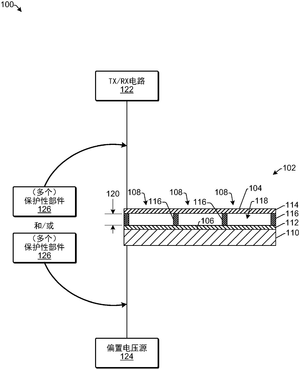
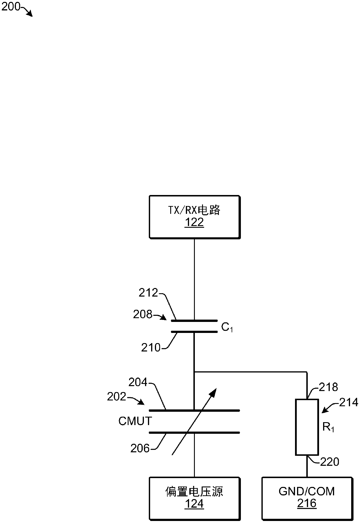
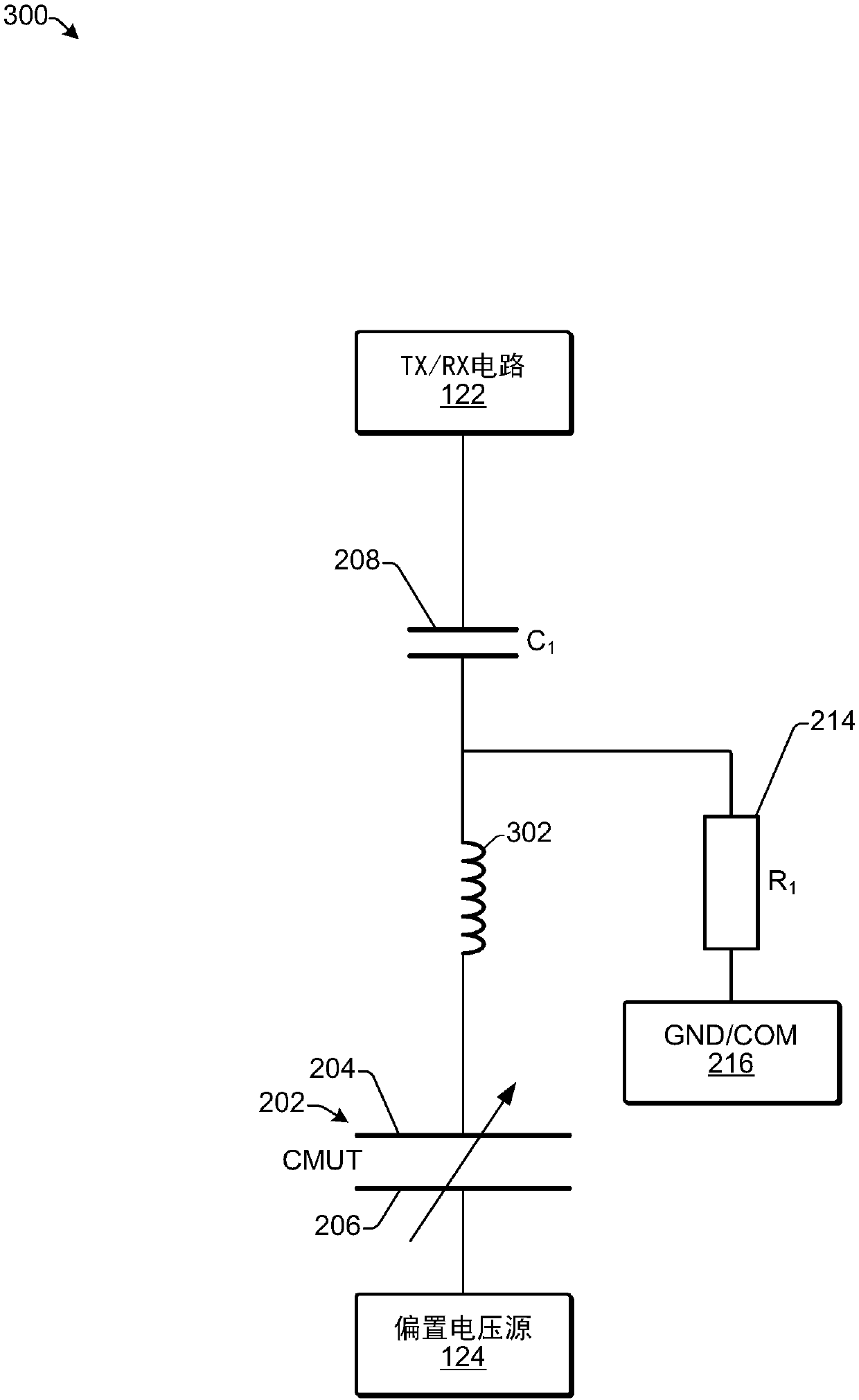
[0025] Some embodiments include techniques and arrangements for applying a bias voltage to a CMUT. Examples of CMUTs to which bias voltages may be applied include: CMUT elements or sub-elements in a CMUT array, one or more CMUT cells in a CMUT system, and/or any other type of CMUT configuration. The CMUT herein may comprise a first electrode opposite the second electrode, wherein there is a transducing gap between the two electrodes. At least one of the electrodes is movable towards and away from the other in order to generate and/or receive ultrasonic energy. A transmit and/or receive (TX/RX) circuit may be electrically connected directly or indirectly to one of the electrodes, and a bias voltage source may be electrically connected directly or indirectly to the other electrode (ie, with or without any other electronic components).
[0026] In embodiments herein, one or more protective components may be included in a circuit between at least one of the electrodes and at least one of a TX/RX circuit or a bias voltage source. As an example, a first capacitor may be placed between the CMUT and the TX/RX circuit to prevent the bias voltage from being directly applied to the TX/RX circuit if the CMUT is damaged. However, if the CMUT is not damaged, the bias voltage is not applied to any circuit portion between the CMUT and the TX/RX circuit, including the first capacitor. The capacitance of the first capacitor may be selected to have minimal effect on the TX/RX signal passing through the first capacitor. For example, the capacitance of the first capacitor may be greater than the capacitance of the CMUT. In some cases, the capacitance of the first capacitor may be approximately 5 times or more greater than the capacitance of the CMUT.
[0027] Additionally, in some examples, a first resistor may be included between the CMUT and the first capacitor for setting the desired DC potential, such as with ground (GND) or a common return path (COM). GND can be earth ground, chassis ground, or signal ground. The resistance of the first resistor may be selected to be greater than the impedance of the CMUT within the operating frequency range of the CMUT. As an example, the resistance of the first resistor may be selected to be approximately 5 times or more greater than the impedance of the CMUT over the operating frequency range of the CMUT. The operating frequency range may be equivalent to a transducer bandwidth (eg, -20dB bandwidth, -40dB bandwidth, etc.) covering all useful signals.
[0028] Also, in some examples, a second capacitor may be placed between the second electrode of the CMUT and GND/COM to reduce noise from the bias voltage source. For example, the capacitance of the second capacitor may be greater than the capacitance of the CMUT. As one example, the capacitance of the second capacitor may be approximately 10 times larger or greater than the capacitance of the CMUT.
[0029] Additionally, in some cases, a second resistor may be positioned between the second electrode of the CMUT and the bias voltage source to protect the bias voltage source if the CMUT is damaged. As an example, the resistance of the second resistor may be smaller than the resistance of the first resistor. For example, the resistance of the second resistor may be about 1/10 to 1/3 of the resistance of the first resistor.
[0030] In some examples, a third capacitor may be connected between the first capacitor and the TX/RX circuit to further protect the TX/RX circuit. Further, a third resistor may be connected between the electrode of the third capacitor connected to the first capacitor and GND/COM. The capacitance of the third capacitor may be similar to the capacitance of the first capacitor, and the resistance of the third resistor may be similar to the resistance of the first resistor.
[0031] In some examples, multiple CMUTs and/or multiple elements in a CMUT may share a common bias voltage source. In this case, the plurality of CMUTs or CMUT elements may share the same second capacitor, and in some cases may share the same second resistor. Additionally, each CMUT or CMUT element may be connected to a separate TX/RX circuit (eg, a separate TX/RX channel in a CMUT system). Each CMUT or CMUT element may include a corresponding first capacitor and (in some examples) a corresponding third capacitor. Further, each CMUT or CMUT element may include a corresponding first resistor and (in some examples) a corresponding third resistor.
[0032] For discussion purposes, some example embodiments are described in the context of ultrasound imaging. However, the embodiments herein are not limited to specific examples, and may be extended to other applications, other systems, other environments for use, other array configurations, etc., as will be apparent to those skilled in the art from the disclosure herein.
[0033] figure 1 An example CMUT system 100 is shown in accordance with some implementations. figure 1 A cross-sectional representation of a CMUT 102 is included, which in some embodiments may have any transducer shape. For example, CMUT 102 may be part of a larger CMUT, part of a CMUT element or sub-element in a CMUT array, or part of any other type of CMUT configuration. In this example, the CMUT 102 includes a first (eg, upper) electrode 104 and a second (eg, bottom) electrode 106 . The first electrode 104 and the second electrode 106 may be flat or otherwise planar in this example, but are not so limited in other examples. Also, although one possible CMUT structure is depicted in this example, the embodiments herein are not limited to the structure shown and can be applied to any CMUT structure having two or more electrodes, where the electrodes At least one of them is movable relative to the other, including CMUTs with embedded springs, etc.
[0034]In the example shown, a plurality of CMUT cells 108 are formed on a substrate 110 . In some cases, the substrate 110 may be formed of a conductive material and may serve as the second electrode 106 of the CMUT cell 108 . In other examples, such as where the substrate 110 is formed of a non-conductive material, a layer of conductive material may be deposited on the upper surface of the substrate 110 to serve as the second electrode 106 , such as prior to depositing the optional insulating layer 112 , which may be An optional insulating layer may be deposited on the upper surface of the second electrode 106 .
[0035] The elastic membrane 114 may be disposed over the substrate 110 and may be supported by the plurality of sidewalls 116 to provide a plurality of cavities 118 respectively corresponding to the individual CMUT cells 108 , eg, one cavity 118 per CMUT cell 108 . In some examples, the membrane 114 may have a uniform thickness over the cavity 118 ; however, in other examples, the thickness or other characteristics of the membrane 114 may vary, which may alter the frequency and/or other characteristics of the CMUT cell 108 . Membrane 114 may be made of a resilient material to enable membrane 114 to move toward and away from substrate 110 within the transduction gap 120 provided by cavity 118 . The membrane 114 may be made of a single layer or multiple layers, and at least one layer may be made of a conductive material to enable the membrane 114 to function as the first electrode 104 .
[0036] Factors affecting the resonant frequency of the CMUT cell 108 include the size of the cavities 118 (corresponding to the area of ​​the membrane above each cavity), and the stiffness of the membrane (which may correspond at least in part to the thickness of the membrane above each cavity 118), Film thickness and film material. Additionally, the structure of the CMUT cells 108 in different regions of the CMUT 102 may be configured differently. For example, the center frequency (or first resonant frequency) of CMUT cells 108 in different regions may be designed differently from CMUT cells 108 in other regions. In some cases, substrate 110 may be bonded or otherwise attached to another substrate not shown in this example (eg, IC wafer/chip, PCB board, glass wafer/chip, acoustic substrate material, etc.).
[0037] The TX/RX circuit 122 may be a front-end circuit that includes a single channel or multiple channels (as further described below) connected to the CMUT or CMUT array 102 to cause the CMUT 102 to transmit ultrasonic energy and/or An electrical signal representative of ultrasonic energy impinging on the CMUT 102 is received. For example, the membrane 114 (as the first electrode 104 ) may be deformed by applying an AC voltage between the first electrode 104 and the second electrode 106 to cause the emission (TX) of ultrasonic energy. Additionally, the membrane 114 may be deformed by impinging ultrasonic waves during reception (RX) of ultrasonic energy. Thus, membrane 114 is capable of moving back and forth within transduction gap 120 in response to an electrical signal when ultrasonic energy is generated or in response to receiving ultrasonic energy.
[0038] The TX/RX circuit 122 may apply an AC (alternating current) electrical signal on the CMUT 102, thereby causing the CMUT 102 to generate ultrasonic waves for transmission operations. Additionally, for receive operations, the TX/RX circuit 122 may receive from the CMUT 102 electrical signals that are acoustically converted by the CMUT 102 . TX/RX circuit 122 may be a front end circuit in system 100 that interfaces with CMUT 102 . Where CMUT 102 is part of a CMUT array, TX/RX circuitry 122 may include TX/RX channels, and each TX/RX channel may have its own TX/RX interfaced with the corresponding CMUT element in the CMUT array front-end circuit. Figure 14 An example of a system with TX/RX circuits/channels 122 is provided. Other types of TX/RX circuits are known in the art.
[0039] A bias voltage source 124 may be connected to the CMUT 102 to apply a bias voltage to the CMUT 102 . A bias voltage (DC or AC voltage) may be applied between electrodes 104 and 106, such as during receive operations. In some cases if the bias voltage source is an AC voltage, the frequency may exceed the operating frequency range of the CMUT such that the bias voltage itself does not cause the CMUT to produce any meaningful acoustic signal. In some cases, the bias voltage source may include a DC-DC converter and one or more bias voltage generators. Examples of bias voltage sources, such as with respect to Figures 15 to 18.
[0040] In some examples, a bias voltage may be applied to CMUT 102 during receive operations. Additionally, or alternatively, a bias voltage may be applied to CMUT 102 during transmit operation. By applying a bias voltage to the CMUT cells 108, electrostatic force loads can be loaded on the membranes 114, which can change the resonant frequency or other characteristics of the corresponding CMUT cells 108. In some cases, by controlling the bias voltage applied to the CMUT 102, at least one CMUT performance parameter (eg, transduction efficiency, frequency response, etc.) can be made different. For example, a bias voltage may be selectively applied to the CMUT 102 to turn on and off the function of the transaxle or to change the performance parameter(s) of the CMUT 102 .
[0041] In some cases, different bias voltages may be applied to different regions of the CMUT 102 (eg, different ones of the CMUT cells 108), thereby assigning different ultrasound receive and/or transmit performance parameters to the different regions. Also, if the bias voltage within a region of the CMUT 102 changes over time, the CMUT performance parameter(s) within that region will also change over time accordingly. As one example, such as where CMUT 102 is included in an array of CMUTs, by controlling the bias voltages in different regions of CMUT 102, the effective aperture and/or apodization of CMUT 102 can be controlled and changed accordingly.
[0042] exist figure 1 In the example of , TX/RX circuit 122 may be connected to a first electrode (eg, 104 ) of CMUT 102 , and bias voltage source 124 may be connected to a second electrode (eg, 106 ) of CMUT 102 . To prevent damage to the TX/RX circuit 122 and/or to the bias voltage source 124, one or more protections may be included between the CMUT 102 and the TX/RX circuit 122, or between the CMUT 102 and the bias voltage source 124 Sexual component 126. refer to below Figure 2 to Figure 12 As additionally described, various electronic components 126 may be included to protect the TX/RX circuit 122 and/or the bias voltage source 124, such as in the event that the CMUT 102 is damaged, malfunctioned, shorted, or the like. Additionally, in some examples, the orientation of CMUT electrodes 104 and 106 may be reversed relative to the electrical connections to TX/RX circuit 122 and bias voltage source 124 .
[0043] figure 2 An example circuit 200 for applying a bias voltage is shown in accordance with some embodiments. The CMUT 202 may be represented in the circuit 200 as a variable capacitor having a first electrode 204 and a second electrode 206 . In some examples, CMUT 202 may correspond to CMUT 102 having first electrode 104 and second electrode 106 discussed above, or other CMUT configurations. For example, CMUT 202 may include multiple CMUT cells, may be elements or sub-elements in a CMUT array, and/or any other desired CMUT structural configuration. Further, circuit 200 may include TX/RX circuit 122 and bias voltage source 124 . Additionally, in some examples, the orientation of CMUT electrodes 204 and 206 may be reversed relative to the electrical connections to TX/RX circuit 122 and bias voltage source 124 .
[0044] The first capacitor C1 208 is electrically connected between the TX/RX circuit 122 and the CMUT 202 and can prevent a bias voltage from being applied directly to the TX/RX circuit 122, such as a short circuit between the first electrode 204 and the second electrode 206 in the case of. In this example, the TX/RX circuit 122 may be connected to the first electrode 204 of the CMUT 202 through the first capacitor C1 208 . The first electrode 210 of the first capacitor C1 208 is connected to the first electrode 204 of the CMUT 202 , and the second electrode 212 of the first capacitor C1 208 is connected to the TX/RX circuit 122 . A bias voltage source 124 (eg, a DC or AC voltage) may be connected to the second electrode 206 of the CMUT 202 .
[0045] Additionally, the first resistor R1 214 is connected to the first electrode 204 of the CMUT 202, the first electrode 210 of the first capacitor C1, and GND/COM 216 (eg, earth ground, chassis ground, AC signal ground, common return path etc.) between. The first electrode 218 of the first resistor R1 214 is connected to the first electrode 204 of the CMUT and the first electrode 210 of the first capacitor 208 . The second electrode 220 of the first resistor 214 is connected to GND/COM 216 .
[0046] The resistance of resistor R1 214 and the capacitance of capacitor C1 208 are both selected to have minimal effect on the TX/RX signal. The capacitance of the first capacitor C1 208 may be greater than the capacitance of the CMUT 202 . In some examples, the capacitance of the first capacitor C1 208 may be approximately 5 times or more greater than the capacitance of the CMUT 202 . In some examples, the capacitance of the first capacitor C1 208 may be approximately 5 times, 10 times, 100 times, 1000 times larger, or greater than the capacitance of the CMUT 202 . For example, the capacitance of CMUT 202 may depend, at least in part, on the size of the CMUT, the size of the CMUT transduction gap, and the like. As an example, the upper limit of the capacitance of the first capacitor C1 208 may depend, at least in part, on component availability by considering voltage ratings and package size in real-world applications. As a non-limiting example, the capacitance of the CMUT in the medical ultrasound probe may be about 5 pF to 100 pF, while the capacitance of the first capacitor may be about 1 nF to 100 nF.
[0047] Also, the resistance of the first resistor R1 214 may be selected to be greater than the impedance of the CMUT 202 over the operating frequency range of the CMUT 202 . In some cases, the resistance of the first resistor R1 214 may be selected to be 5 times or more greater than the impedance of the CMUT 202 over the operating frequency range of the CMUT. In some examples, the resistance of the first resistor R1 214 may be selected to be 5 times, 10 times, 100 times, 1000 times, or greater than the impedance of the CMUT 202 over the operating frequency range of the CMUT. The operating frequency range of the CMUT 202 may be equivalent to the transducer bandwidth (eg, -20dB bandwidth, -40dB bandwidth, etc.) covering the desired signal. Also, the insulating layer of CMUT 202 (corresponding to, eg, insulating layer 112 of CMUT 102 ) may have finite resistance, so the upper limit of first resistor R1 214 may be 5 to 10 times lower than the resistance of the insulating layer of CMUT 202 .
[0048] exist figure 2In the example shown in, under normal operation, the CMUT 202 separates the bias voltage source 124 from the TX/RX circuit 122 so that normally no bias voltage is applied to the TX/RX circuit 122 or to the CMUT 202 and TX /RX circuit 122 between any components. Additionally, when applying the bias voltage, if there is a short circuit in the CMUT 202 , the bias voltage may be applied across the first capacitor C1 208 rather than across the first capacitor C1 208 across the TX/RX circuit 122 . Also, resistor R1 214 prevents the bias voltage from being shorted directly to GND/COM 216 so that bias voltage source 124 can maintain the bias voltage (or otherwise operate normally) even when there is no short circuit in CMUT 202 . For example, when multiple CMUTs share the same bias voltage source 124, if there is a short circuit in one CMUT, the bias voltage can still be maintained on the other CMUTs that share the bias voltage source. Thus, when there is a short circuit in the CMUT 202, the first capacitor C1 208 and the second resistor R1 214 combine to protect the TX/RX circuit 122 and keep the bias circuit functioning properly.
[0049] image 3 An example circuit 300 for applying a bias voltage to a CMUT is shown in accordance with some embodiments. In this example, the circuit 300 includes a first capacitor C1 208 and a first resistor R1 214 connected to GND/COM 216 . Further, the circuit 300 includes an inductor 302 that may be included anywhere along the signal path between the TX/RX circuit 122 and the CMUT 202 . For example, inductor 302 may be used to tune the performance of CMUT 202 by matching the impedance difference between CMUT 202 and interface circuits, which may include cables, other conductors, and/or TX/RX circuits ( image 3 not shown).
[0050] As one example, the impedance of the CMUT 202 (over its operating frequency range) may be much higher than the impedance of the cable, other conductors, and/or TX/RX circuits. Thus, the inductor 302 can be used to tune the impedance of the CMUT 202 to better match the impedance of the cable or other conductors to improve the efficiency of the system. For example, the inductance of the inductor may be selected such that the resonant frequency of the inductor and the CMUT (eg, modeled as a capacitor) is in the range from 0.1Fc to 5Fc (where Fc is the center frequency of the CMUT). In some cases, the inductor 302 may be placed close to the CMUT 202 . For example, the inductor 302 may be connected between the CMUT 202 and the first capacitor 208 . exist Figure 1 to Figure 13 In any of the configurations shown in , an inductor 302 may optionally be added within the line between the TX/RX circuit and the CMUT.
[0051] Figure 4 An example circuit 400 for applying a bias voltage to a CMUT is shown in accordance with some embodiments. In this example, the circuit 400 includes a first capacitor C1 208 and a first resistor R1 214 . However, the first resistor R1 214 is connected in parallel with the first capacitor 208 instead of being connected to ground. Accordingly, the first electrode 210 of the first capacitor 208 is connected to the second electrode 220 of the first resistor 214 and the second electrode 212 of the first capacitor 208 is connected to the first electrode 218 of the first resistor 214 . In the event of a short circuit in the CMUT 202 , the bias voltage may be applied across both the first resistor and the first capacitor instead of the TX/RX circuit 122 . Additionally, the DC voltage potential at the first electrode 210 of the first capacitor C1 208 may be defined based on the DC potential of the second electrode 212, which may be defined by the TX/RX circuit.
[0052] Figure 5 An example circuit 500 for applying a bias voltage to a CMUT is shown in accordance with some embodiments. In this example, the circuit 500 includes a first capacitor C1 208 and a first resistor R1 214 connected to GND/COM 216 . Additionally, the circuit 500 includes a second capacitor C2502. The first electrode 504 of the second capacitor 502 is connected to the second electrode 206 of the CMUT 202 , and the second electrode 506 of the second capacitor C2 502 is connected to the GND 216 . The capacitance of the second capacitor 502 may improve the noise performance of the bias voltage by reducing the noise caused by the bias voltage source 124 . For example, the capacitance of the second capacitor C2 502 may be greater than the capacitance of the CMUT 202 . In some examples, the capacitance of the first capacitor C2 502 may be 5 times or greater than the capacitance of the CMUT 202 . In some examples, the capacitance of the first capacitor C2 502 may be 5 times, 10 times, 100 times, 1000 times larger, or greater than the capacitance of the CMUT 202 .
[0053] Image 6 An example circuit 600 for applying a bias voltage to a CMUT is shown in accordance with some embodiments. In this example, the circuit 600 includes a first capacitor C1 208 and a first resistor R1 214 connected to GND/COM 216 . Additionally, the circuit 600 includes a second capacitor 502 connected to the second electrode 206 of the CMUT 202 and to the GND 216 . Also, the circuit 600 includes a second resistor R2 602 having a first electrode 604 connected to the first electrode 504 of the second capacitor 502 and the second electrode 206 of the CMUT 202 . The second electrode 606 of the second resistor R2 602 may be connected to the bias voltage source 124 . In some examples, the second resistor R2 602 is optional.
[0054] The second resistor T2 602 can protect the bias voltage source 124 from large AC signals from the TX/RX circuit 122 if the CMUT 202 is damaged, shorted, etc. For example, the resistance of the second resistor R2 602 may be less than the resistance of the first resistor R1 214. For example, the resistance of the second resistor R2 602 may be 1/10 to 1/3 the resistance of the first resistor R1 214 . In addition, in some cases, the impedance of the second resistor R2 602 may be greater than the impedance of the second capacitor C2 502 in the CMUT operating frequency range, such as 5 times larger than the impedance of the second capacitor C2 502 in the CMUT operating frequency range or larger. As an example, the impedance of the second resistor R2 602 is 5 times, 10 times, 100 times greater, or greater than the impedance of the second capacitor C2 502 over the CMUT operating frequency range.
[0055] Figure 7 An example circuit 700 for applying a bias voltage to a CMUT is shown in accordance with some embodiments. In this example, the circuit 700 includes a first capacitor C1 208 and a first resistor R1 214 connected to GND/COM 216 . Additionally, the circuit 700 includes a second capacitor C2 502 and a second resistor R2 602 connected in parallel. Thus, the first electrode 604 of the second resistor 602 is electrically connected to the first electrode of the second capacitor and the second electrode 206 of the CMUT 202 . Additionally, the second electrode 606 of the second resistor 602 is connected to the second electrode 506 of the second capacitor 502 and the bias voltage source 124 . As mentioned above, the capacitance of the second capacitor C2 502 may be greater than the capacitance of the CMUT 202 . In some examples, the capacitance of the first capacitor C2 502 may be approximately 5 times or greater than the capacitance of the CMUT 202 . In some examples, the capacitance of the first capacitor C2 502 may be approximately 5 times, 10 times, 100 times, 1000 times larger, or greater than the capacitance of the CMUT 202 . Further, within the CMUT operating frequency range, the second resistor R2 602 may have a resistance between 1/10 and 1/3 the resistance of the first resistor R1 214, and/or the second resistor R2 602 may have An impedance that is 5 times, 10 times, 100 times greater, or greater than the impedance of the second capacitor C2 502 .
[0056] Figure 8 An example circuit 800 for applying a bias voltage to a CMUT is shown in accordance with some embodiments. In this example, the circuit 800 includes a first capacitor C1 208 and a first resistor R1 214 connected to GND/COM 216 as a first resistor-capacitor (RC) stage 802 . Thus, the first RC stage 802 includes a circuit consisting of the first resistor R1 214 and the first capacitor C1 208 . Furthermore, the circuit 800 includes the TX/RX circuit 122 , and a second RC stage 804 electrically connected between the first RC stage 802 and the TX/RX circuit 122 . The second RC stage 802 includes a third resistor R3 806 and a third capacitor C3 808 . The first electrode 810 of the third capacitor C3 808 is electrically connected to the second electrode 212 of the first capacitor C1 208 and the first electrode 812 of the third resistor 806 . The second electrode 814 of the third capacitor C3 808 is connected to the TX/RX circuit 122 . The second electrode 816 of the third resistor 806 is connected to GND/COM 216 . Additionally, the circuit 800 includes a second capacitor 502 connected to GND/COM 216 and a second resistor 602 connected between the bias voltage source 124 and the CMUT 202 .
[0057] The capacitance of the third capacitor C3 808 may be similar in value to the capacitance of the first capacitor C1 208, for example, the capacitance of the third capacitor C3 808 may be 5 times, 10 times, 100 times, 1000 times greater, or greater than the capacitance of the CMUT 202 . Also, the resistance value of the third resistor R3 806 may be similar to the resistance value of the first resistor R1 214, eg, the resistance of the third resistor R3 806 may be selected to be greater than the resistance value of the CMUT 202 over the operating frequency range of the CMUT 202 202 impedance. For example, the resistance of the third resistor R3 806 may be 5 times, 10 times, 100 times, 1000 times greater, or greater than the impedance of the CMUT 202 over the operating frequency range.
[0058] The second RC stage 804 may be connected anywhere between the first RC stage 804 and the TX/RX circuit 122 . Also, the second RC stage 802 may be included in Figure 3 to Figure 7 in any of the circuit configurations shown in . As an example, in the event that the CMUT 202 is shorted and the first capacitor C1 208 is also shorted, the second RC stage can protect the TX/RX circuit 122 from damage by the bias voltage source 124, and thus can be used in medical applications or the like it works.
[0059] Figure 9 An example configuration of a circuit 900 of an ultrasound system including a plurality of CMUTs to which bias voltages are applied is shown in accordance with some embodiments. E.g, Figure 2 to Figure 8 The circuit configuration in is described relative to a CMUT, such as multiple CMUT cells, or elements or sub-elements in a CMUT array. However, Figure 2 to Figure 8 The circuit configuration can be applied to systems that include multiple CMUTs, such as multiple CMUT elements, multiple subelements, or bias-controllable regions in an array of CMUTs. In this example, such as in the case of a CMUT array, multiple CMUT elements, sub-elements or bias controllable regions may share the same bias voltage source 124 . For example, CMUT arrays can be classified into three or more different array types consisting of multiple CMUT elements, including one-dimensional (1D) arrays, one-and-a-half-dimensional (1.5D) arrays, and two-dimensional (2D) arrays . For example, a 1D array may include CMUT elements arranged in only one dimension (eg, the lateral dimension). The spacing between two adjacent elements can typically be either one wavelength for a linear array or half a wavelength for a phased array. A 1.5D array may include multiple elements in the lateral dimension and at least two sub-elements in the height dimension. A 2D array may include multiple elements arranged in both lateral and height dimensions. Examples of CMUT arrays are described in US Patent Application No. 14/944,404, filed November 18, 2015, and US Patent Application No. 15/212,326, filed July 18, 2016, the entire disclosures of which are incorporated herein by reference .
[0060] Figure 9An example of a circuit 900 is shown, the system includes a system based on Image 6 The bias voltage application configuration for the plurality of CMUTs 202(1), 202(2), . . . , 202(N) of the circuit configuration in . In some examples, the plurality of CMUTs 202( 1 )-202(N) may each be separate elements or sub-elements in the CMUT array and/or may share the same bias voltage source 124 . The second electrodes 206 of the plurality of CMUTs 202(1) to 202(N) are electrically connected to each other to form a common electrode of the plurality of CMUTs 202(1) to 202(N). The bias voltage source 124 may be connected directly or indirectly to the second electrode 206 . In this example, a second resistor R2 602 (in some examples, R2 may be optional) is electrically connected between the bias voltage source 124 and the respective plurality of CMUTs 202(1)-202(N) between the two electrodes 206 . Additionally, the first electrode 504 of the second capacitor C2 502 is electrically connected to the second electrode 206 of the plurality of CMUTs 202(2)-202(N), and the second electrode 506 of the second capacitor C2 502 is connected to GND/ com 216.
[0061] Additionally, the first electrode 204 of each CMUT 202(1)-202(N) may be connected to separate TX/RX circuits 122(1), 122(2), . . . , 122(N), in some examples, The TX/RX circuits may be front-end circuits for individual channels of the ultrasound system. further, as in figure 2 In an example of , a corresponding first capacitor C1 208 and a corresponding first resistor R1 214 connected to GND/COM 216 may be connected between the CMUTs 202(1)-202(N) and the corresponding TX/RX circuit 122(1 ) to 122(N). Thus, each CMUT 202(1)-202(N) may be connected to a corresponding first capacitor 208, a corresponding first resistor 214, and a corresponding TX/RX circuit 122(1)-122(N), and The plurality of CMUTs may share connections to the bias voltage source 124 , the second capacitor 502 , and the second resistor 602 . Further, the configuration of circuit 900 may be only one of a variety of circuits 900 that may be employed in a CMUT array, such as where different bias voltages are applied to different parts of the array. For example, the first circuit 900 may be applied to a first set of elements or sub-elements in an array, or a first bias controllable region (eg, a region of a CMUT cell with independently controllable bias voltages to assign different characteristics to different regions), and likewise the second circuit 900 can be applied to a second set of elements or sub-elements in the array, or to a second bias controllable region to enable application of different bias voltages with different amounts of voltage and or at different timing to apply the different bias voltages.
[0062] Additionally, multiple CMUTs 202(1), 202(2), . . . , 202(N) may be grouped into multiple groups. The multiple CMUTs in each group may share the same bias voltage source 124 . The bias voltage sources 124 for each respective group may be different. Further, each set of CMUTs may include multiple CMUT elements, CMUT sub-elements, or may be bias-controllable CMUT regions (regions of CMUT cells with independently controllable bias voltages to assign different characteristics to different regions). Each CMUT (eg, a CMUT element, sub-element, or other CMUT region) of the plurality of CMUTs in each group may have a corresponding first capacitor and a corresponding first resistor, and each group may have a corresponding first capacitor and a corresponding first resistor. A corresponding second capacitor C2 502 and (optionally) a corresponding second resistor R2 602 .
[0063] Figure 10 An example configuration of a circuit 1000 of an ultrasound system including a plurality of CMUTs to which bias voltages are applied is shown in accordance with some embodiments. For example, in this example, Figure 8 The circuit configuration of the can be applied to a system that includes multiple CMUTs, such as multiple CMUT elements or subelements in an array of CMUTs. Thus, circuit 1000 may be included in a system in which bias voltages may be applied to a plurality of CMUTs 202(1), 202(2), . . . , 202(N). In some examples, the plurality of CMUTs 202( 1 )-202(N) may each be separate elements or sub-elements in the CMUT array and/or may share the same bias voltage source 124 . The second electrodes 206 of the plurality of CMUTs 202(1) to 202(N) are electrically connected to each other to form a common electrode of the plurality of CMUTs 202(1) to 202(N). The bias voltage source 124 may be connected directly or indirectly to the second electrode 206 . In this example, a second resistor R2 602 (which may be optional in some cases) is electrically connected between the bias voltage source 124 and the respective plurality of CMUTs 202(1)-202( N) between the second electrodes 206. Additionally, the first electrode 504 of the second capacitor C2 502 is electrically connected to the second electrode 206 of the plurality of CMUTs 202(2)-202(N), and the second electrode 506 of the second capacitor C2 502 is connected to GND/COM 216.
[0064] Additionally, the first electrode 204 of each CMUT 202(1)-202(N) may be connected to separate TX/RX circuits 122(1), 122(2), . . . , 122(N), in some examples, The TX/RX circuit may be a separate channel of the TX/RX circuit. further, as in figure 2 In the example of a corresponding first capacitor C1 208 and a corresponding first resistor R1 214 connected to GND/COM 216 may be connected between the CMUTs 202(1)-202(N) and the corresponding TX/RX circuit 122(1) to 122(N). Additionally, a corresponding third capacitor C3 808 and a third resistor R3 806 connected to GND/COM 216 are also connected between the corresponding TX/RX circuits 122(1)-122(N) and each corresponding CMUT 202(1 ) to 202(N) and between.
[0065] Thus, each CMUT 202(1)-202(N) may be connected to a corresponding first capacitor 208, a corresponding first resistor 214, and a corresponding TX/RX circuit 122(1)-122(N), and The plurality of CMUTs may share connections to the bias voltage source 124 , the second capacitor 502 , and the second resistor 602 . Further, the configuration of circuit 1000 may be only one of a variety of circuits 1000 that may be employed in a CMUT array, such as where different bias voltages are applied to different parts of the array. For example, the first circuit 1000 can be applied to a first group of elements or subelements in an array, and likewise the second circuit 1000 can be applied to a second group of elements or subelements in the array to enable the application of different voltages with different amounts of voltage The bias voltage and or the different bias voltages are applied at different times.
[0066] Figure 9 and Figure 10 The configuration shown in the circuit with multiple CMUTs is based on Image 6 and Figure 8 configuration shown in . above relative to Figure 2 to Figure 5 and Figure 7 The other circuit configurations discussed can similarly be implemented with multiple CMUTs.
[0067] Figure 11 An example configuration of an ultrasound probe system 1100 including one or more CMUTs is shown in accordance with some embodiments. In this example, the ultrasound probe system 1100 includes a connector 1102 that interfaces with one or more TX/RX circuits 122 and is connected to the probe handle 1104 through one or more conductors 1106 . The one or more conductors 1106 may include coaxial cables or other types of cables, wires, wires, etc., to provide an electrical connection between the probe handle and the connector 1102 . In some cases, the one or more conductors 1106 may be a cable bundle, which may include multiple coaxial cables, multiple pairs of wires, multiple pairs of leads, or the like.
[0068] The detector handle may include an acoustic window 1108 and a CMUT 1110. In some cases, the one or more conductors 1106 may be flexible, allowing the user to freely manipulate the probe handle 1104. For example, the probe handle 1104 can be designed to be light and small. Accordingly, in some examples herein, the number of components in the probe handle 1104 may be minimized to facilitate placement of the components in the connector 1102 . Accordingly, protective components such as the first capacitor C1 and the first resistor R1 and/or other protective components may be included in the connector 1102 . Specifically, since each TX/RX circuit (eg, each system channel) may include a pair of first capacitor C1 and first resistor R1 , and in some cases, there may be a large number of channels, the detector handle 1104 Including these components substantially increases the size of the probe handle 1104 .
[0069] As an example, assume that CMUT 1110 is a CMUT array with a large number of CMUT elements, and thus a large number of first capacitors and first resistors, eg, one pair per CMUT element. Additionally, based on Figure 2 to Figure 10 An example circuit of a large number of capacitors and resistors may be included in an ultrasound probe system having such a large number of CMUT elements. However, if the probe handle 1104 includes a large number of capacitors and resistors as protective components, the handle 1104 can be significantly increased in size and weight compared to a handle 1104 without protective components. Accordingly, based on Figure 2 to Figure 10 The example circuits discussed in, in some examples, capacitors 208, 502, 808, and/or resistor(s) 214, 602, 806 (eg, as Figure 11 not shown in Figure 2 to Figure 10 shown in one or more of ) may be located within the connector 1102 instead of the probe handle 1104. Additionally, or alternatively, as discussed below, the second capacitor 502 and/or the optional second resistor 602 may be located within the probe handle 1104 or at another suitable location in the system 1100 .
[0070] Figure 12 An example configuration of an ultrasound probe system 1200 including one or more CMUTs is shown in accordance with some embodiments. Example detector system 1200 illustrates one possible configuration of detector system 1100 in which at least some of the protective components are included within connector 1102 . Figure 12 An example corresponds to image 3 circuit 300, but Figure 2 to Figure 10 Other circuits in the circuits described in can be similarly configured in the detector system 1200. In the example shown, the first capacitor 208 and the first resistor 214 are located in the connector 1102 . In some examples, respective inductors 302 may be included or may be positioned within probe handle 1104 in proximity to respective CMUTs 202 in order to tune respective CMUTs 202 . right figure 2 and Figure 4 to Figure 10 A similar implementation can be used for the circuit configuration.
[0071] Additionally, a bias voltage source 124 may be positioned in the ultrasound system 1200 (as shown) and connected to the connector 1102 . Bias voltage source 124 may alternatively be positioned within connector 1102 . As another alternative, a bias voltage source may be housed within the detector handle 1104 . The bias voltage source 124 may have the ultrasound system 1200, a battery, or other power source ( Figure 12 not shown in) the power provided.
[0072] Figure 13 An example configuration of an ultrasound probe system 1300 including multiple CMUTs is shown in accordance with some embodiments. As one example, CMUTs 202(1)-202(N) may be included within a CMUT array, and may correspond, for example, to CMUT elements or sub-elements in the CMUT array, respectively. Example detector system 1300 illustrates one possible configuration of a detector system in which at least some of the protective components are included within connector 1102 . Figure 13 An example corresponds to image 3 The circuit 300 with Figure 9 a combination of circuit 900, but figure 2 , Figure 4 to Figure 8 and Figure 10 Other circuits in the circuits described in can be similarly configured in the detector system 1300.
[0073] In the example shown, a plurality of first RC stages 802(1)-802(N) (including first capacitor C1 208 and first resistor R1 214) are located in connector 1102 and communicate with one or more TX/ RX circuitry 122 communicates, in some examples, the TX/RX circuitry includes multiple TX/RX channels. Since there may be relatively few second capacitors C2 502 and second resistors R2 602 for each array (in some examples, there may be only one pair of second capacitors 502 and second resistors 602 for a normal ID array, or for There may be a pair for each bias controllable region or sub-element in the 1.5D array), the second capacitor C2 502 and the second resistor R2 602 may be located in the connector 1102, the probe handle 1104, or a other locations. The second capacitor C2 502 , and optional second resistor R2 602 are located within the connector 1102 in the example shown and are in communication with the bias voltage source 124 .
[0074] The plurality of CMUTs 202(1)-202(N) are seated in the probe handle 1104. In some examples, the respective inductors 302 may be included or may be positioned within the probe handle 1104 in proximity to the respective CMUTs 202 to which they are tuned. Figure 10 Embodiments of the Detector System 1300 may be similarly incorporated. Bias voltage source 124 may be positioned in ultrasound system 1300 (as shown) and connected to connector 1102 . Alternatively, the bias voltage source 124 may be positioned within the connector 1102 . As another alternative, the bias voltage source 124 may be housed within the detector handle 1104 . The bias voltage source 124 may have the ultrasound system 1300, a battery, or other power source ( Figure 13 not shown in) the power provided.
[0075] Figure 14 is a block diagram illustrating an example configuration of an ultrasound system 1400 that includes one or more CMUTs, according to some embodiments. In this example, system 1400 includes one or more CMUTs 1402 . In some cases, CMUT 1402 may correspond to the above with respect to Figure 1 to Figure 13 At least one of the CMUTs 102 or 202 in question. System 1400 further includes imaging system 1406 , multiplexer 1408 , and bias voltage source 1410 in communication with CMUT 1402 . As a non-limiting example, the system 1400 may include or may be included in an ultrasound probe device for performing ultrasound imaging, as described above with respect to Figure 11 to Figure 13 discussed.
[0076] Further, system 1400 may include multiple TX/RX channels 1412. For example, CMUT 1402 may include 128 (eg, N) transmit and receive channels 1412 in communication with multiplexer 1408 . In some examples, characteristics of at least some of the CMUTs 1402 may vary and may be altered by changing the bias voltage provided to the CMUTs 1402 . Further, in some cases, the physical configuration of the CMUT cells within CMUT 1402 may vary, which may also change the transmit and receive characteristics of different bias controllable regions.
[0077] Additionally, as indicated at 1416 , the bias voltage source 1410 may generate one or more bias voltages to apply to the one or more CMUTs 1402 . Further, in some examples, the generated bias voltage may be time-dependent and may vary over time.
[0078] Imaging system 1406 may include one or more processors 1418 , one or more computer-readable media 1420 , and a display 1422 . For example, processor(s) 1418 may be implemented as one or more physical microprocessors, microcontrollers, digital signal processors, logic circuits, and/or other devices that manipulate signals based on operational instructions. Computer-readable media 1420 may be tangible non-transitory computer storage media and may include any type of data structures, program modules, or processor-executable instructions, data structures, program modules, or processor-executable instructions, data structures, or volatile and non-volatile memory, computer storage devices, and/or removable and non-removable media implemented by technology. Further, when referred to herein, non-transitory computer readable media exclude media such as energy, carrier signals, electromagnetic waves, and the signals themselves.
[0079] In some examples, imaging system 1406 may include, or may be connectable to, display 1422 and/or various other input and/or output (I/O) components, such as for visualization of signals received by CMUT 1402 . Additionally, imaging system 1406 may communicate with multiplexer 1408 through multiple TX/RX channels 1424. Furthermore, imaging system 1406 may be in direct communication with multiplexer 1408, eg, in addition to being in communication with bias voltage source 1410 (as indicated at 1426), for controlling a plurality of switches therein (as indicated at 1428) ).
[0080] Multiplexer 1408 may include a number of high voltage switches and/or other multiplexing components. Embodiments herein may be used for any number of channels 1424 , any number of channels 1412 , and any number of CMUTs 1402 . The one or more CMUTs 1402 may use the above with respect to Figure 1 to Figure 13 Any of the circuit configurations discussed are connected to bias voltage source 1410 and/or TX/RX channel 1412 .
[0081] Figure 15 is a block diagram illustrating an example of selected components of bias voltage source 1410 according to some embodiments. The bias voltage source 1410 may include a DC-DC converter 1502 and one or more bias voltage generators 1506 . The DC-DC converter 1502 of the bias voltage source 1410 can convert the low DC voltage 1508 (eg, 5V, 10V, etc.) to a high DC voltage such as 200V, 400V, etc. In some examples, the bias voltage generator 1506 may generate a monotonically increasing bias voltage 1510 for the one or more CMUTs 1402, such as after receiving a start signal. For example, the bias voltage 1510 may increase over time, as discussed additionally below. Furthermore, in some examples, the bias voltage generator 1506 may reduce the level of the bias voltage 1510 to an initial voltage (eg, 0V) relatively quickly after receiving the end signal or at a predetermined time. Bias voltage generator 1506 may be implemented using at least one of analog or digital counting.
[0082] Figure 16 An example of a bias voltage generator 1506 is shown in accordance with some embodiments. The bias voltage generator 1506 in this example may be an analog bias voltage generator and includes a first switch K 1 1602, the first resistor R a 1604, a capacitor C1606 connected to ground/common 1608, and a second switch K 2 1612 is connected to the second resistor R of ground/common 1608 b 1610. When the first switch K 1 When 1602 is closed, the voltage V supplied to the bias voltage generator 1506 DC 1614 begins to charge capacitor C 1606, and the bias voltage V 偏置 1510 at rate (1-e -t/τ ) increases exponentially, where τ=R a C is the time constant. As an example, after the ultrasonic signal reaches a predetermined depth, the first switch K may be turned on 1 1602 and can close the second switch K 2 1612. This allows when capacitor C 1606 passes through resistor R b 1610 Bias voltage V when discharging 偏置 The 1510 quickly drops to 0V. In some cases, the second resistor R b 1610 can have a ratio resistor R a 1604 significantly smaller resistance. In addition, opening and closing the first switch K 1 1602 and the second switch K 2 Control signals 1616 and 1618 of 1612 may be determined by the above with respect to Figure 14 The processor 1418 of the imaging system in question, or generated by a separate timing device within the system. The timing means may be analog or digital.
[0083] Figure 17 An example of a bias voltage generator 1506 is shown in accordance with some embodiments. The bias voltage generator 1506 in this example may be an analog bias voltage generator and includes a first switch K 1 1702, the first resistor R z 1704, capacitor C 1706, and a second switch K accessible through 2 1710 A second resistor R connected in parallel with capacitor C 1706 y 1708. Additionally, the bias voltage generator 1506 includes an amplifier 1712 having a first connection 1714 , a second connection 1716 to ground/common 1718 , and a third connection 1720 . The voltage V may be provided to the bias voltage generator 1506 DC 1722. Amplifier 1712 creates an integrating circuit such that when the first switch K 1 When 1702 is closed, the bias voltage V 偏置 1510 begins to increase linearly at rate t/τ, where τ=R z C is the time constant. As an example, after the ultrasonic signal reaches a predetermined depth, the first switch K may be turned on 1 1702 and can close the second switch K 2 1710, which allows when capacitor C 1706 passes through the second resistor R y 1708 V when discharging 偏置 The 1510 drops quickly to 0V. In some cases, the second resistor R y 1708 can have a ratio resistor R z 1704 significantly smaller resistance. In addition, the control signals 1724 and 1726 can open and close the first switch K, respectively 1 1702 and the second switch K 2 1710, and can be determined by the above with respect to Figure 14 The processor 1418 of the imaging system 1406 in question, or generated by a separate timing device within the system. The timing means may be analog or digital.
[0084] Although two analog examples of bias voltage generator 1506 are described herein, similar principles can be extended to other analog circuits capable of generating variable voltage outputs, as will be apparent to those skilled in the art having the benefit of the disclosure herein. . Further, in some examples, as mentioned above, a digital version of the bias voltage generator 1506 may be employed.
[0085] Figure 18An example of a bias voltage generator 1506 is shown in accordance with some embodiments. In this example, bias voltage generator 1506 may be a digital bias voltage generator and may include digital waveform generator 1802 , digital-to-analog converter 1804 , and high voltage amplifier 1806 . Digital waveform generator 1802 receives start signal 1808 and begins outputting a digital waveform at 1810. A digital-to-analog converter 1804 converts the digital waveform 1810 to an analog voltage signal 1812 . Then, the high voltage amplifier 1806 scales the analog voltage signal 1812 to the desired bias voltage level, thereby generating the bias voltage 1510 . As an example, after the ultrasound signal reaches a predetermined depth, a stop signal may be sent to the digital waveform generator 1802, which causes V 偏置 1510 drops to 0V. can be compared from the above Figure 14 The processor 1418 of the imaging system 1406 in question, or by a separate timing device internal to the system, generates the clock signal 1814 for controlling the digital waveform generator 1802. The timing means may be analog or digital.
[0086] Figure 19 is a flow diagram illustrating an example process in accordance with some implementations. The processes are shown as a collection of blocks in a logic flow diagram, the collection of blocks representing a sequence of operations. The order in which the blocks are described should not be construed as limiting. Any number of the described blocks may be combined in any order and/or in parallel to implement a process or alternative processes, and not all blocks need to be performed. For purposes of discussion, the processes are described with reference to the apparatuses, architectures, and systems described in the examples herein, although the processes may be implemented in a variety of other apparatuses, architectures, and systems.
[0087] Figure 19 is a flow diagram illustrating an example process 1900 for applying a bias voltage to a CMUT in accordance with some embodiments. The processes may be performed, at least in part, by a processor programmed or otherwise configured with executable instructions.
[0088] At 1902, the first electrode of the first capacitor may be electrically connected to the first electrode of the CMUT. As an example, the capacitance of the first capacitor may be 5 times or greater than the capacitance of the CMUT. Other suitable ranges discussed above.
[0089] At 1904, the second electrode of the first capacitor may be electrically connected to transmit and/or receive (TX/RX) circuitry.
[0090] At 1906, the first electrode of the first resistor may be electrically connected to the first electrode of the CMUT and the first electrode of the first capacitor. For example, the resistance of the first resistor may be 5 times or more greater than the impedance of the CMUT within the operating frequency range of the CMUT. Other suitable ranges discussed above.
[0091] At 1908, the second electrode of the first resistor may be electrically connected to at least one of: (1) a ground or common return path, or (2) the second electrode of the first capacitor.
[0092] At 1910, the first electrode of the second capacitor may be electrically connected to the second electrode of the CMUT. Further, the second electrode of the second capacitor may be electrically connected to ground and/or a common return path. As an example, the capacitance of the second capacitor may be 5 times or greater than the capacitance of the CMUT. Other suitable ranges discussed above.
[0093] At 1912, the first electrode of the second resistor may be electrically connected to the first electrode of the second capacitor and the second electrode of the CMUT, and the second electrode of the second resistor may be electrically connected to the bias voltage source. In some examples, the resistance of the second resistor may be 1/10 to 1/3 the resistance of the first resistor over the CMUT operating frequency range, and/or the impedance of the second resistor may be greater than that of the second capacitor The impedance is 5 times larger or more. Other suitable ranges discussed above.
[0094] At 1914, the first electrode of the third capacitor may be electrically connected to the second electrode of the first capacitor. For example, the capacitance of the third capacitor may be 5 times or more larger than the capacitance of the CMUT. Other suitable ranges discussed above.
[0095] At 1916, the second electrode of the third capacitor may be electrically connected to the TX/RX circuit.
[0096] At 1918, the first electrode of the third resistor may be electrically connected to the first electrode of the third capacitor and the second electrode of the first capacitor. As an example, the resistance of the third resistor may be 5 times or more greater than the impedance of the CMUT over the operating frequency range of the CMUT. Other suitable ranges discussed above.
[0097] At 1920, the second electrode of the third resistor may be electrically connected to at least one of: (1) a ground or common return path, or (2) the second electrode of the third capacitor.
[0098] At 1922, a bias voltage may be applied to the second electrode of the CMUT at least during the period during which the CMUT is receiving ultrasonic energy. For example, when the second resistor is present, the applied bias voltage may pass through the second resistor to the second electrode of the CMUT. As one example, a processor in the system may cause the CMUT to transmit and/or receive ultrasound energy when a bias voltage is applied to the second electrode of the at least one CMUT. In some cases, a first bias voltage may be applied to the first CMUT and a second bias voltage may be applied to the second CMUT. Further, in some examples, at least one of the first bias voltage or the second bias voltage may be applied as an increasing bias voltage that increases over time.
[0099] The example procedures described herein are merely examples of procedures provided for discussion purposes. Numerous other variations will be apparent to those skilled in the art from the disclosure herein. Further, although the disclosure herein presents several examples of suitable systems, architectures, and apparatus for performing the processes, the embodiments herein are not limited to the specific examples shown and discussed. Furthermore, the present disclosure provides various example embodiments, as described and illustrated in the accompanying drawings. However, the present disclosure is not limited to the embodiments described and shown, but may extend to other embodiments, as will or will become known to those skilled in the art.
[0100] Although the subject matter has been described in language specific to structural features and/or methodological acts, it is to be understood that the subject matter defined in the appended claims is not necessarily limited to the specific features or acts described. Rather, the specific features and acts are disclosed as example forms of implementing the claims.

PUM

no PUM

Description & Claims & Application Information

We can also present the details of the Description, Claims and Application information to help users get a comprehensive understanding of the technical details of the patent, such as background art, summary of invention, brief description of drawings, description of embodiments, and other original content. On the other hand, users can also determine the specific scope of protection of the technology through the list of claims; as well as understand the changes in the life cycle of the technology with the presentation of the patent timeline. Login to view more.
Why Eureka
Try Eureka