Array substrate, display panel and display device

A technology of array substrate and substrate substrate, which is applied to instruments, nonlinear optics, optics, etc., can solve the problems of large metal bending angle, reduced picture contrast, increased dark state brightness, etc., to reduce the impact, improve dark state light leakage, The effect of improving the display quality

Active Publication Date: 2021-07-09
WUHAN TIANMA MICRO ELECTRONICS CO LTD
View PDF11 Cites 0 Cited by
  • Summary
  • Abstract
  • Description
  • Claims
  • Application Information

AI Technical Summary

Problems solved by technology

The existence of via holes in the data lines causes the boundary conditions of the data lines at the via holes to change due to etching residues, causing the boundaries of the data lines at the via holes to be circular or elliptical, forming a large metal corner , resulting in light leakage
When the alignment of the array substrate and the color filter substrate deviates, the light leakage will shift to the light-transmitting area, which increases the brightness of the dark state and reduces the contrast of the screen.

Method used


Image

  • Array substrate, display panel and display device
  • Array substrate, display panel and display device
  • Array substrate, display panel and display device

Examples


Embodiment Construction

[0029] The following will clearly and completely describe the technical solutions in the embodiments of the present invention with reference to the accompanying drawings in the embodiments of the present invention. Obviously, the described embodiments are only some, not all, embodiments of the present invention. Based on the embodiments of the present invention, all other embodiments obtained by persons of ordinary skill in the art without creative efforts fall within the protection scope of the present invention.

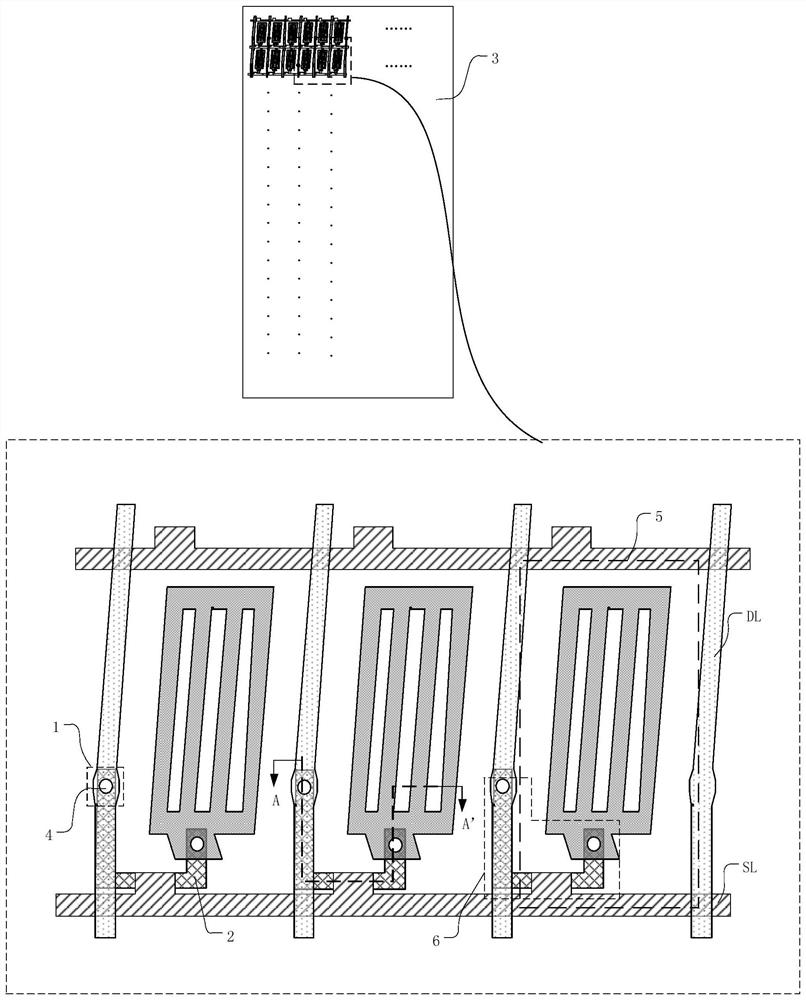
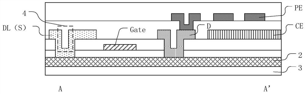
[0030] This embodiment provides an array substrate, please refer to figure 1 and figure 2 , figure 1 is a schematic top view of an array substrate provided by an embodiment of the present invention, figure 2 is along figure 1 A schematic diagram of a cross-sectional structure along the line AA'. The array substrate includes: a base substrate 3; a plurality of scan lines SL and a plurality of data lines DL formed on the base substrate 3, and a plurality of sca...


PUM


Abstract

The invention discloses an array substrate, a display panel and a display device. The array substrate includes: a base substrate; a plurality of scan lines and a plurality of data lines formed on the base substrate; a plurality of scan lines and a plurality of data lines are insulated to define a plurality of sub-pixel units; the sub-pixel units include thin film transistors, data The line is electrically connected to the active layer of the thin film transistor through the via hole; the data line includes an anti-leakage structure, and the anti-leakage structure includes a first transition part, a middle part and a second transition part; the first transition part includes two along the extending direction of the data line. One end face of the first transition part along the extending direction of the data line is connected to the middle part; the second transition part includes two end faces along the extending direction of the data line, and one end face of the second transition part along the extending direction of the data line is connected to the middle part catch. The invention can improve the light leakage in the dark state of the via hole and improve the picture quality without affecting the transmittance.

Description

technical field [0001] The present invention relates to the field of display technology, in particular to an array substrate, a display panel and a display device. Background technique [0002] A Liquid Crystal Display (LCD) is one of the most widely used flat panel displays. The LCD is provided with an array substrate, a color filter substrate, and a liquid crystal layer arranged between the two substrates. The array substrate is provided with structures such as scan lines, data lines, thin film transistors, pixel electrodes, and common electrodes. [0003] In the prior art, thin film transistors are generally used as switching devices in pixel units to control on and off of pixel electrodes. The data line is electrically connected to the active layer of the thin film transistor through the via hole. When the data line has a large bend angle (generally greater than 10°), light leakage will occur. The existence of via holes in the data lines causes the boundary condition...

Claims


Application Information

Patent Timeline
Patent Type & Authority Patents(China)
IPC IPC(8): G02F1/1362
CPCG02F1/136286
Inventor 陈宝玲马扬昭吴玲沈柏平
Owner WUHAN TIANMA MICRO ELECTRONICS CO LTD
Why Eureka
Try Eureka