Double layer superposed electronic paper driving structure

A driving structure, electronic paper technology, applied in instruments, static indicators, etc., can solve the problems of cumbersome hardware system and unsightly structure, and achieve the effect of optimizing the test interface, increasing the display effect, and simplifying the hardware structure

Pending Publication Date: 2018-04-06
DALIAN LONGNING TECH
0 Cites 0 Cited by

AI-Extracted Technical Summary

Problems solved by technology

[0002] In recent years, as people's visual pursuit of electronic display effects has become higher and higher, the research and application of color electronic paper has gradually attracted more and more people's attention. Generally, the upper and lower layers of electronic paper belong to two independent and different types of electronic pa...

Method used

As shown in Figure 1, the upper floor electronic paper test interface is directly or indirectly connected with the second drive layer FPC8 of the lower floor electronic paper that partially exposes the metal pad surface through the first driving layer FPC4; as shown in Figure 2, the lower floor electronic paper The test interface is directly or indirectly connected to the first driving layer FPC4 of the upper e-paper with a partially exposed metal pad surface through the second driving...

Abstract

The present invention provides a double-layer stacked electronic paper drive structure, which is characterized in that it includes an upper layer of electronic paper, which is a cholesteric liquid crystal electronic paper screen, mainly composed of a front glass substrate, a bottom glass substrate, a first drive control chip, a first drive The first layer of FPC and the liquid crystal and plastic frame inside the LCD screen; the first drive control chip is located on the bottom glass substrate; the lower layer of electronic paper is electrophoretic electronic paper, mainly composed of electrophoretic electronic paper film, back glass substrate, second driver The control chip and the second driving layer FPC are composed; the second driving control chip is located on the back glass substrate; the test interface of the upper layer electronic paper/lower layer electronic paper directly or indirectly communicates with the double layer through the respective first driving layer FPC/second driving layer FPC The stacked electronic paper test system boards are connected together, and the surroundings of the double stacked electronic paper driving structure are sealed with a sealant. The invention has the advantages of increasing display effect, optimizing test interface, simplifying hardware structure, reducing cost and the like.

Application Domain

Static indicating devices

Technology Topic

Electronic band structureEngineering +3

Image

  • Double layer superposed electronic paper driving structure
  • Double layer superposed electronic paper driving structure

Examples

  • Experimental program(1)

Example Embodiment

[0021] In order to make the objectives, technical solutions, and advantages of the embodiments of the present invention clearer, the technical solutions in the embodiments of the present invention will be described clearly and completely in conjunction with the accompanying drawings in the embodiments of the present invention. Obviously, the described embodiments It is a part of the embodiments of the present invention, not all the embodiments. Based on the embodiments of the present invention, all other embodiments obtained by those of ordinary skill in the art without creative work shall fall within the protection scope of the present invention.
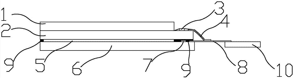
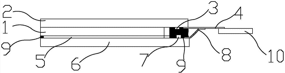
[0022] Such as figure 1 , figure 2 As shown, a double-layer superimposed electronic paper drive structure includes:
[0023] The upper e-paper is a cholesteric liquid crystal e-paper screen, and can also use an electronic control structure unit with reflection function or absorption of primary color light. After power-on, the transparent e-paper display mode is electrowetting mode, horizontal electrophoresis technology mode or The electrochromic mode is mainly composed of the surface glass substrate 1, the bottom glass substrate 2, the first drive control chip 3, the first drive layer FPC4, and the liquid crystal and plastic frame inside the liquid crystal screen; the first drive control chip 3 is located On the bottom glass substrate 2;
[0024] The lower layer of electronic paper is electrophoretic electronic paper, which can be used to switch between black and white and red and grayscale. It is mainly composed of electrophoretic electronic paper film 5, back glass substrate 6, second drive control chip 7 and second drive Layer FPC8; the second drive control chip 7 is located on the back glass substrate 6;
[0025] When the upper layer of electronic paper and the lower layer of electronic paper are superimposed, under normal circumstances, in order to make the edge of the double-layer superimposed electronic paper as small as possible, the first drive control chip 3 and the second drive control chip 7 are located on the same side. good. The installation method of the first drive control chip 3 or the second drive control chip 7 is COG or COF.
[0026] When the thickness of the second driving control chip 7 of the lower electronic paper is smaller than that of the electrophoretic electronic paper film 5, the bottom glass substrate 2 of the upper electronic paper is on the bottom or the surface glass substrate 1 of the upper electronic paper is on the bottom, it can be used figure 1 Or the structure of 2; when the thickness of the second drive control chip 7 of the lower layer of electronic paper is greater than that of the electrophoretic electronic paper film 5, the face glass substrate 1 of the upper layer of electronic paper is below, that is, only figure 2 Structure. When the surface glass substrate 1 of the upper electronic paper is underneath, the total thickness of the surface glass substrate 1 and the electrophoretic electronic paper film 5 should not exceed 0.7 mm. The upper/lower e-paper is bonded through the OCA (Optically Clear Adhesive) of the e-paper film surface of the lower e-paper.
[0027] Such as figure 1 As shown, the upper electronic paper test interface is directly or indirectly connected to the lower electronic paper second driving layer FPC8 with the metal pad surface partially exposed through the first driving layer FPC4; figure 2 As shown, the lower electronic paper test interface is directly or indirectly connected to the upper electronic paper first driving layer FPC4 with the metal pad surface partially exposed through the second driving layer FPC8. The first driving layer FPC4/the second driving layer FPC8 are both double-sided special-shaped structures. The double-sided special-shaped structure means that the shape of the driving layer FPC is "one", "L" or "U". and many more. In order to prevent the transmission of low-frequency signals from being affected by DC impedance, the FPC of the drive layer should avoid unnecessary turns, and try to use arc connections at the corners to shorten the transmission distance.
[0028] The test interfaces of the upper layer of electronic paper/the lower layer of electronic paper are finally all connected to the double-layer stacked electronic paper test system board 10. The above-mentioned connection method can be hot pressing, welding or other connection methods. The surroundings of the double-layer superimposed electronic paper drive structure are sealed by a sealant 9. The sealant 9 is made of epoxy resin, and its water absorption rate is less than 0.5%, and the water vapor permeability is less than 4g/(m 2 ·24h), the test condition of water vapor permeability is 60℃/90%RH, the sample thickness is 1mm, and finally enter the high-pressure chamber for defoaming and drying.
[0029] E-paper superimposed in this way can not only increase the display effect, but also optimize the test interface, simplify the hardware structure of the test system, and play an important role in reducing costs.
[0030] Finally, it should be noted that the above embodiments are only used to illustrate the technical solutions of the present invention, but not to limit them; although the present invention has been described in detail with reference to the foregoing embodiments, those of ordinary skill in the art should understand: It is still possible to modify the technical solutions described in the foregoing embodiments, or equivalently replace some or all of the technical features; and these modifications or replacements do not make the essence of the corresponding technical solutions deviate from the technical solutions of the embodiments of the present invention. range.

PUM

no PUM

Description & Claims & Application Information

We can also present the details of the Description, Claims and Application information to help users get a comprehensive understanding of the technical details of the patent, such as background art, summary of invention, brief description of drawings, description of embodiments, and other original content. On the other hand, users can also determine the specific scope of protection of the technology through the list of claims; as well as understand the changes in the life cycle of the technology with the presentation of the patent timeline. Login to view more.

Similar technology patents

Realization method for electronic dynamic travel notes

InactiveCN104699382Aavoid disproportionImprove the display effect
Owner:上海携图信息科技有限公司

Interactive method and terminal device

Owner:GREE ELECTRIC APPLIANCES INC OF ZHUHAI

Bidirectional three-dimensional display device

InactiveCN103838030AAvoid color castImprove the display effect
Owner:TRULY SEMICON

Grating film and three-dimensional display device

InactiveCN106959483AImprove screen flickeringImprove the display effect
Owner:NINGBO THREDIM OPTOELECTRONICS CO LTD

Classification and recommendation of technical efficacy words

  • Improve the display effect

Shift register and drive method thereof, gate drive circuit and display device

ActiveCN104900268Astable signalImprove the display effect
Owner:WUHAN TIANMA MICRO ELECTRONICS CO LTD +1

Touch display screen and touch display device

ActiveCN102955303AAvoid electrostatic damageImprove the display effect
Owner:BEIJING BOE OPTOELECTRONCIS TECH CO LTD

Picture display method and apparatus

InactiveCN105183308AImprove the display effectReduce traffic resource waste
Owner:NUBIA TECHNOLOGY CO LTD
Why Eureka
Try Eureka