A manufacturing method of a low-power fast switch plastic-encapsulated high-voltage silicon stack and a high-voltage silicon stack

A high-voltage silicon stack, fast switching technology, used in semiconductor/solid-state device manufacturing, semiconductor devices, electrical components, etc., can solve problems such as surface corrosion and product surface roughness, achieve high reverse withstand voltage, small welding pore area, Achieve high performance pickling effect

Inactive Publication Date: 2019-07-02
SHANDONG UNIV OF TECH
View PDF4 Cites 0 Cited by
  • Summary
  • Abstract
  • Description
  • Claims
  • Application Information

AI Technical Summary

Problems solved by technology

[0010] In the current conventional formula of mixed acid, the surface of some products is rough after pickling, and it will cause a considerable proportion of surface corrosion pits

Method used


Image

  • A manufacturing method of a low-power fast switch plastic-encapsulated high-voltage silicon stack and a high-voltage silicon stack
  • A manufacturing method of a low-power fast switch plastic-encapsulated high-voltage silicon stack and a high-voltage silicon stack

Examples


Embodiment Construction

[0072] The technical content of the present invention is described below through specific specific embodiments, and those skilled in the art can easily understand other advantages and effects of the present invention from the content disclosed in this specification. The present invention can also be implemented or applied through other different specific embodiments, and various modifications and changes can be made to the details in this specification based on different viewpoints and applications without departing from the spirit of the present invention.

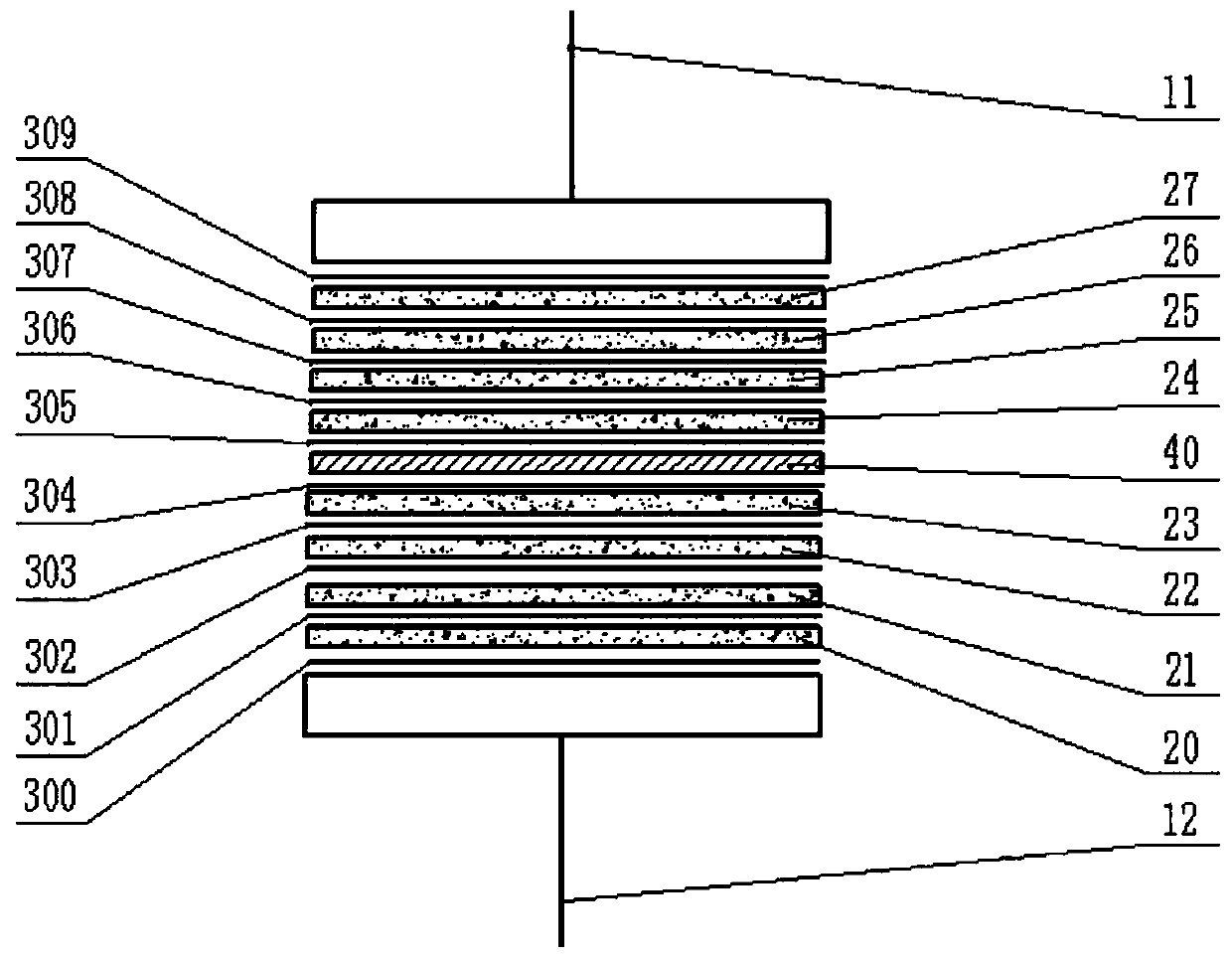
[0073] A method for manufacturing a low-power fast switch plastic-encapsulated high-voltage silicon stack, comprising the following steps:

[0074] Step 1: Preparation of Diode Die

[0075] To avoid ambiguity and facilitate understanding, the diode grain mentioned here is a basic component for making a high-voltage silicon stack, and may also be called a die or a chip or a diode silicon chip. They have the same structure...


PUM


Abstract

The invention discloses a manufacturing method of a high voltage silicon rectifier stack with low power consumption and quick switching and plastic packaging and the high voltage silicon rectifier stack. The manufacturing method disclosed by the invention comprises the steps of diode crystalline grain preparation, switch tube preparation, filling, welding, washing and packaging. By using differentcoefficients of thermal expansion and shape changes of crystalline grains and soldering lugs at high temperature, automatic pulling for the crystalline grains after welding can be realized without the need of aligning the crystalline grains in advance before welding, the air hole area is greatly reduced, the welding quality is improved, and the electrical yield of the crystalline grains after acid pickling of a mixed acid prepared from hydrofluoric acid, acetic acid, sulfuric acid and nitric acid in a volume ratio of 8.8: 13: 5.6: 9.2 is high. Measured data indicates that the forward voltageof the silicon rectifier stack cannot exceed 8 V when the backward voltage is 10000 V under the condition that other parameters are not influenced, and effective turning-off can be realized within extremely time of 17 ns, so that the high frequency rectification problem at high voltage and low power consumption is solved.

Description

technical field [0001] The invention belongs to the field of high-voltage silicon stacks, and in particular relates to a method for manufacturing high-voltage silicon stacks with low power consumption and fast switching plastic-encapsulated high-voltage silicon stacks. [0002] method and the resulting high-voltage silicon stack. Background technique [0003] With the development of power electronics technology, the application technology of high-voltage, high-frequency and high-power devices has been widely upgraded, and correspondingly, the requirements for low-power fast switching high-voltage silicon stacks are getting higher and higher. For example, high-definition color TVs and plastic-encapsulated silicon stack products for displays are developing towards high speed (ultra-fast recovery), high reliability, and miniaturization. Energy saving and emission reduction have special significance. [0004] However, the reverse voltage, forward voltage and switching speed of...

Claims


Application Information

Patent Timeline
Patent Type & Authority Patents(China)
IPC IPC(8): H01L21/50H01L25/11
CPCH01L21/50H01L25/117
Inventor 李昊阳刘云燕赵栋孙美玲王琨琨魏功祥付圣贵
Owner SHANDONG UNIV OF TECH
Why Eureka
Try Eureka