Organic light-emitting device structure and internal temperature monitoring method

A technology of organic light-emitting devices and organic devices, which is applied in the directions of measuring instrument components, instruments, measuring electricity, etc., and can solve the problems of difficult real-time monitoring, complex equipment, and low test accuracy.

Active Publication Date: 2018-04-10
GUAN YEOLIGHT TECH CO LTD
View PDF5 Cites 0 Cited by
  • Summary
  • Abstract
  • Description
  • Claims
  • Application Information

AI Technical Summary

Problems solved by technology

[0004] At present, most rely on external thermometers (such as scanning temperature microscope (SThM), Raman spectroscopy, etc.) to detect the temperature of the screen, which is affected by the thermal conductivity of the screen glass interface. To achieve high-precision measurement, it is also necessary to be equipped with relevant alignment and focusing devices; on the other hand, the equipment is complex and difficult to monitor in real time, which needs to be improved urgently

Method used


Image

  • Organic light-emitting device structure and internal temperature monitoring method
  • Organic light-emitting device structure and internal temperature monitoring method
  • Organic light-emitting device structure and internal temperature monitoring method

Examples


Embodiment 1

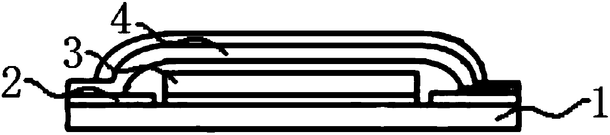
[0032] Please refer to figure 1 , this embodiment specifically discloses a specific structure of an organic light emitting device.

[0033] The structure of the organic light emitting device includes: a substrate 1 , electrodes 2 and organic devices 3 formed on the substrate 1 , and a packaging structure.

[0034] The substrate 1, the electrodes 2 formed on the substrate 1 and the organic device 3 are the basic components of the organic light-emitting device, which can realize that the organic material will emit light when a current passes through, that is, it has the characteristic of self-luminescence.

[0035] The encapsulation structure is the key component structure in this embodiment, which includes at least three layers and one of them is an inorganic semiconductor layer 4. Based on this design, when a certain area of ​​the organic light-emitting device generates a higher temperature, the excessively high The temperature of the inorganic semiconductor layer will affect...

Embodiment 2

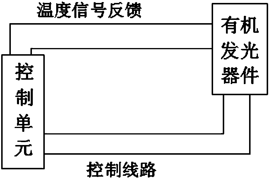
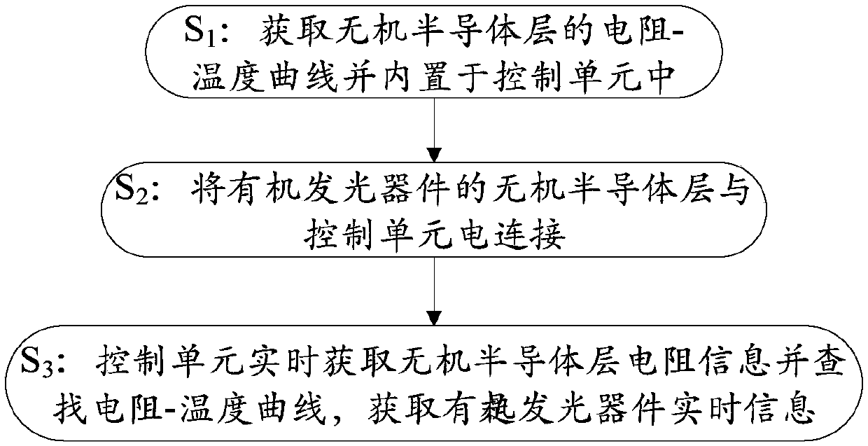
[0044] see figure 2 and image 3 , this embodiment specifically discloses a method for monitoring the internal temperature of an organic light emitting device.

[0045] The method for monitoring the internal temperature of an organic light-emitting device specifically includes the following steps:

[0046] S1: Obtain the resistance-temperature curve of the inorganic semiconductor layer and build it into the control unit;

[0047] S2: electrically connecting the inorganic semiconductor layer of the organic light-emitting device described in Embodiment 1 to the control unit;

[0048] S3: the control unit obtains the resistance information of the inorganic semiconductor layer in real time and searches for the resistance-temperature curve, and obtains real-time information of the organic light-emitting device.

[0049] see Figure 5 A set of resistance-temperature curve example diagrams are given. This figure shows an example of the temperature curve when the inorganic penins...


PUM


Abstract

The invention discloses an organic light-emitting device structure, which comprises a substrate, an electrode, an organic device and a package structure, wherein the electrode and the organic device are formed on the substrate. The package structure comprises at least three layers, wherein one layer is an inorganic semiconductor layer. The inorganic semiconductor layer and the organic device are separated by at least one layer of insulation layer. The inorganic semiconductor layer is electrically connected to the external portion of the package structure. Through the design above, when some area of the organic light-emitting device has higher temperature, excessively high temperature will influence actual resistance of the inorganic semiconductor layer; and by continuously measuring resistance of the inorganic semiconductor layer through a control unit, and by searching a resistance-temperature curve of the inorganic semiconductor layer, a real-time temperature value, that is, an internal temperature value of the organic light-emitting device, of the inorganic semiconductor layer can be obtained.

Description

technical field [0001] The present disclosure generally relates to the technical field of electronic display, and specifically relates to a structure of an organic light-emitting device and a method for monitoring its internal temperature. Background technique [0002] OLED (Organic Light-Emitting Diode), also known as organic light-emitting diode, its basic principle is to use very thin organic material coating and glass substrate, when there is current passing through, the organic material will emit light, that is, its Has self-luminous properties. Different from the traditional LCD display method, it does not need a backlight, which can save power. In addition, the OLED display screen can be made lighter and thinner, and the viewing angle is wider. However, although OLED has the above advantages, at the current stage, organic light-emitting display technology still has defects such as short service life and difficulty in enlarging the screen. [0003] In terms of short ...

Claims


Application Information

Patent Timeline
Patent Type & Authority Applications(China)
IPC IPC(8): G09G3/3208G01R31/00G01D11/00
Inventor 郭立雪朱映光谢静胡永岚
Owner GUAN YEOLIGHT TECH CO LTD
Why Eureka
Try Eureka