Storage control FPGA-based FLASH bad block simulation verification system

A technology of storage control and simulation verification, applied in design optimization/simulation, special data processing applications, instruments, etc., to achieve the effect of improving simulation verification coverage and strong developability

Active Publication Date: 2018-04-20
SHANGHAI SPACEFLIGHT INST OF TT&C & TELECOMM
View PDF4 Cites 3 Cited by
  • Summary
  • Abstract
  • Description
  • Claims
  • Application Information

AI Technical Summary

Problems solved by technology

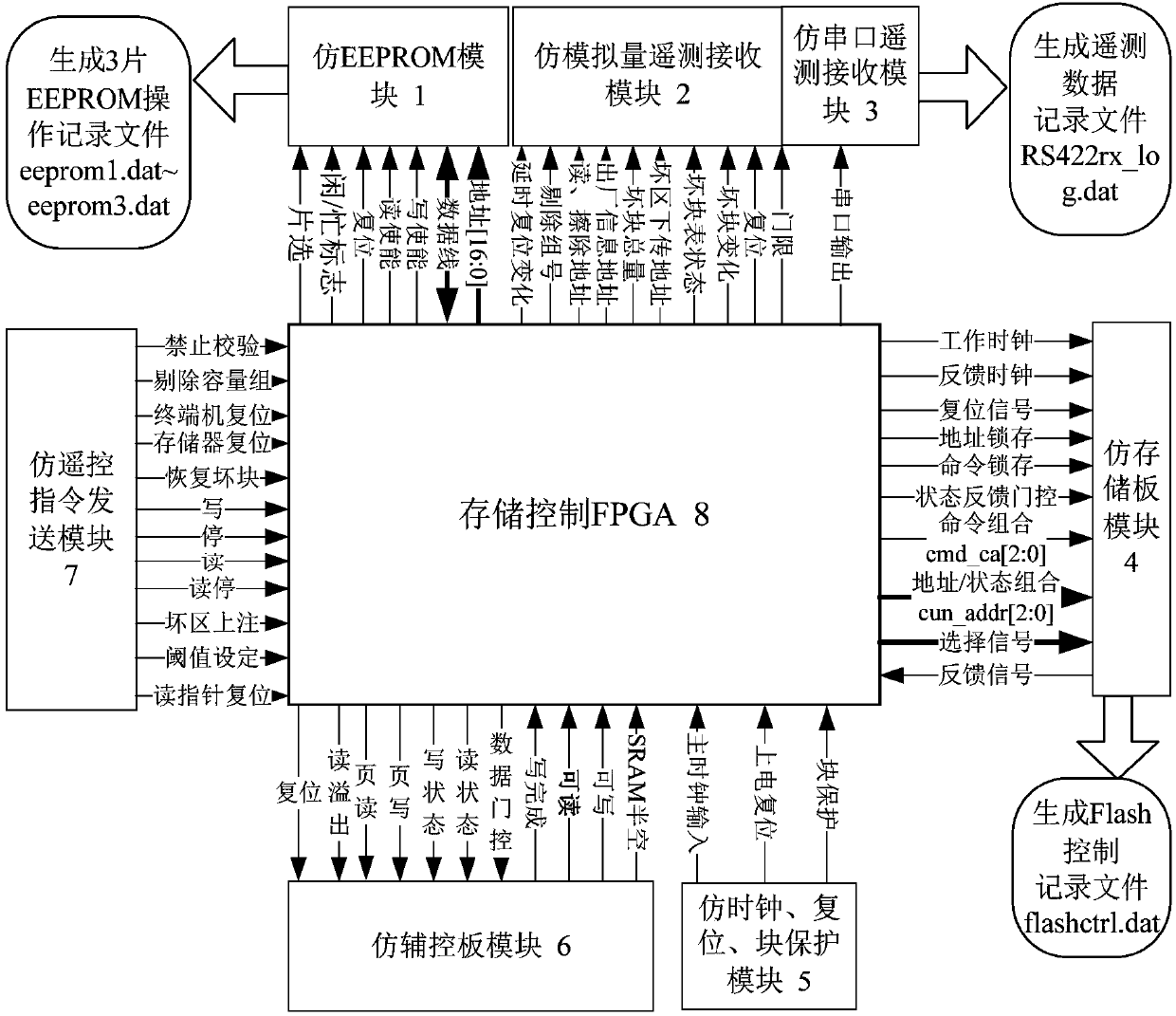
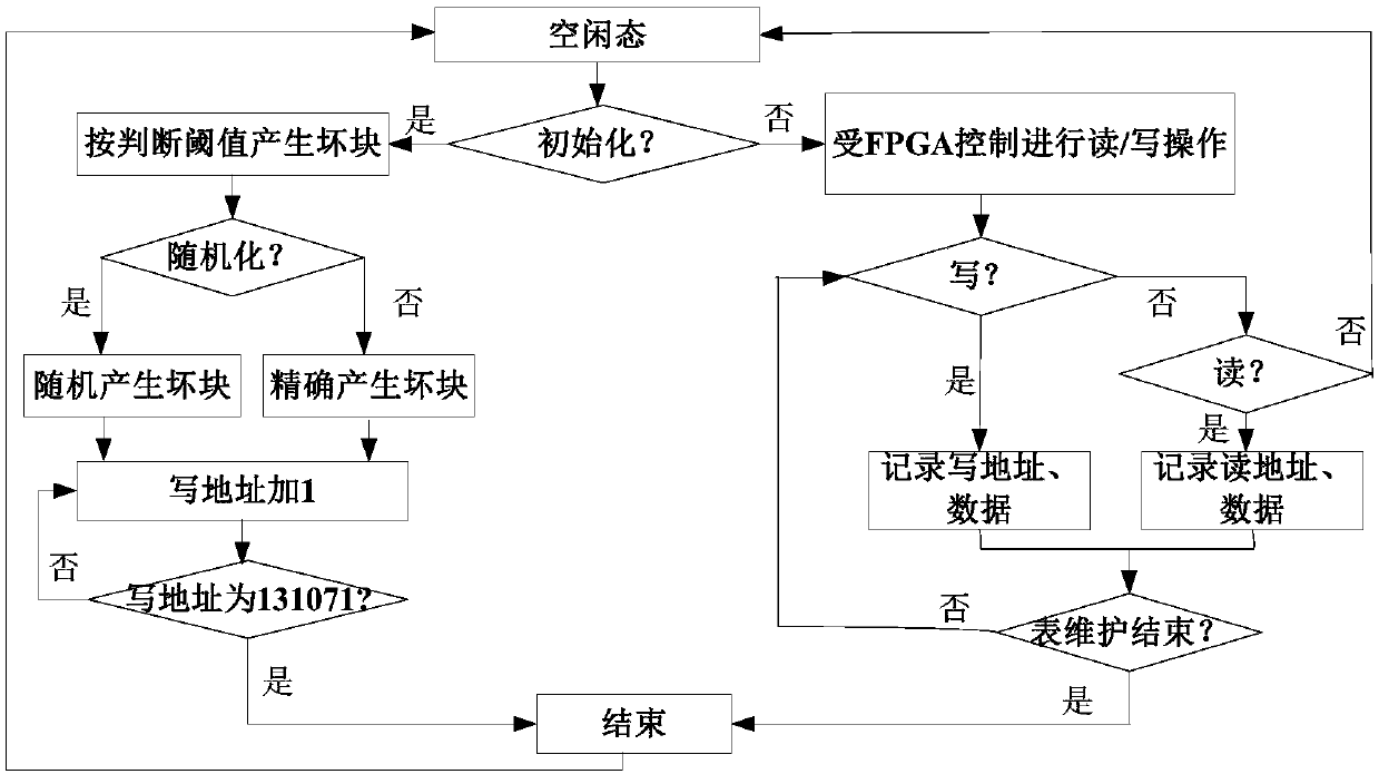
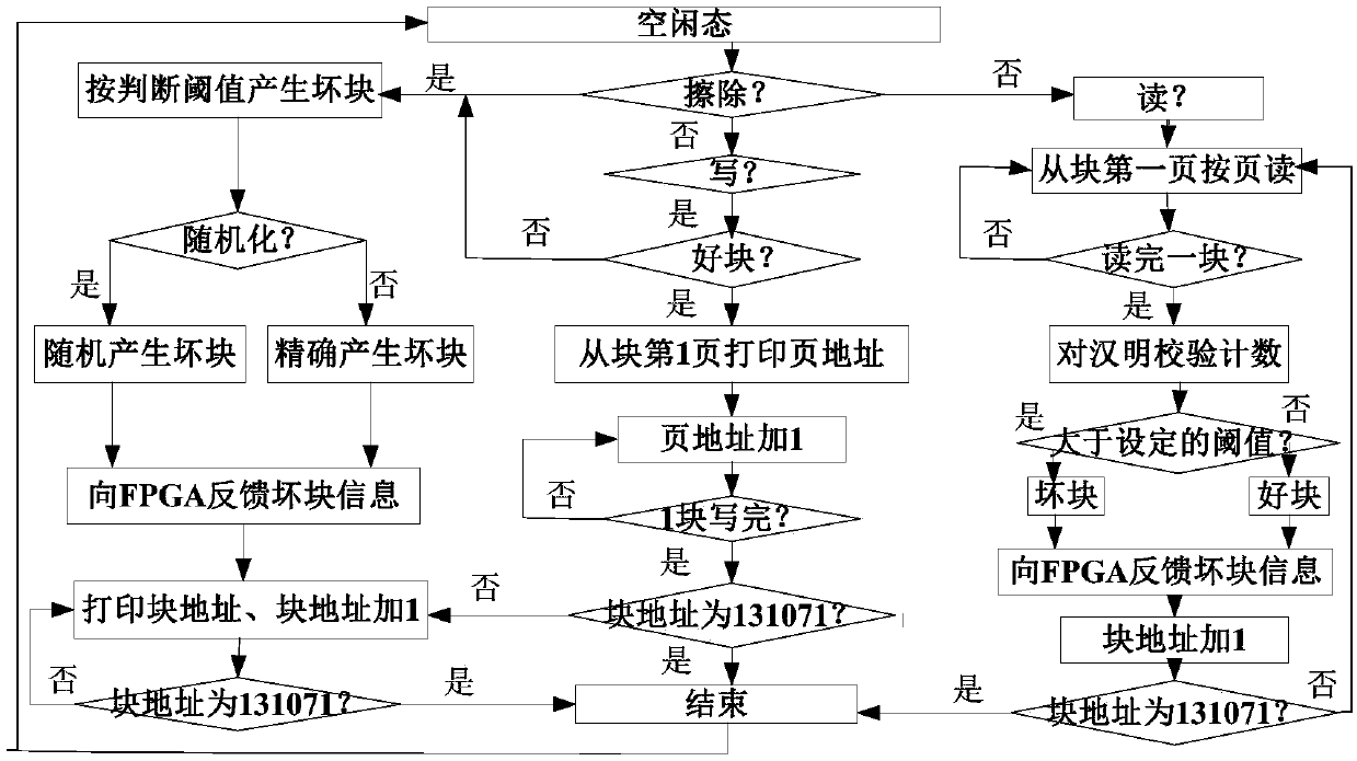
[0004] The purpose of the present invention is to provide a FLASH bad block simulation verification system based on storage control FPGA, to solve the establishment and maintenance of the initial bad block table, the factory bad block table, and the working bad block table of the storage technology in the existing satellite engineering , Establish a mechanism for FLASH in the storage board to perform erasing and reading operations and to feed back bad block information to the storage control FPGA

Method used


Image

  • Storage control FPGA-based FLASH bad block simulation verification system
  • Storage control FPGA-based FLASH bad block simulation verification system
  • Storage control FPGA-based FLASH bad block simulation verification system

Examples


Embodiment Construction

[0030] The technical solutions in the embodiments of the present invention will be clearly and completely described and discussed below in conjunction with the accompanying drawings of the present invention. Obviously, what is described here is only a part of the examples of the present invention, not all examples. Based on the present invention All other embodiments obtained by persons of ordinary skill in the art without creative efforts fall within the protection scope of the present invention.

[0031] In order to facilitate the understanding of the embodiments of the present invention, specific embodiments will be taken as examples for further explanation below in conjunction with the accompanying drawings, and each embodiment does not constitute a limitation to the embodiments of the present invention.

[0032] This embodiment provides a FLASH bad block simulation and verification system based on a storage control FPGA, which is used to provide a closed-loop working envir...


PUM


Abstract

The invention provides a storage control FPGA-based FLASH bad block simulation verification system. The system comprises a simulated EEPROM module, a simulated analog quantity telemetry receiving module, a simulated serial port telemetry receiving module, a simulated storage board module, a simulated clock, a reset module, a block protection module, a simulated auxiliary control board module and asimulated remote control instruction sending module. The system is suitable for ground simulation verification of a storage control FPGA in a satellite product. Bad blocks can be generated in any position by changing a code analog storage board (based on a FLASH) of a simulation system; and the correctness of the storage control FPGA under various working conditions can be verified. Meanwhile, aworking process of a bad block table also can be recorded; various remote control instructions can be input to the storage control FPGA in a simulated manner; telemetry information is received and stored; and a closed-loop simulation environment is provided for the storage control FPGA. The system can be expanded and applied to storage control FPGA ground simulation verification of multiple typesof satellite products.

Description

technical field [0001] The invention relates to solid-state memory in satellite products, in particular to ground simulation of a solid-state memory comprehensive processor system, which is mainly used in the technical field of large-capacity solid memory design, and in particular to a FLASH bad block simulation verification system based on storage control FPGA. Background technique [0002] Solid-state memory (solid storage) based on FLASH is widely used in satellite engineering as a storage device. The advantages of FLASH are low power consumption, low cost, and no loss of data when power is turned off. The disadvantage is that it is limited by the chip process and cannot guarantee reliable performance within its life cycle. For this reason, it is necessary to design storage control FPGA to manage bad blocks of FLASH in satellite products. However, due to the randomness of the effective storage unit FLASH bad blocks in the storage board, it is difficult to accurately set ...

Claims


Application Information

Patent Timeline
Patent Type & Authority Applications(China)
IPC IPC(8): G06F17/50
CPCG06F30/20
Inventor 刘国斌金臻左丽丽祝周荣姜丽梅吴维林刘伟
Owner SHANGHAI SPACEFLIGHT INST OF TT&C & TELECOMM
Why Eureka
Try Eureka