Appearance inspection apparatus for semiconductor assembly, and optical path structure thereof

A technology of appearance inspection and optical path, which is applied in the direction of optical testing for flaws/defects, material analysis through optical means, scientific instruments, etc., and can solve problems such as increasing equipment installation and calibration time, and increasing manufacturers' troubles

Active Publication Date: 2018-05-01
KING YUAN ELECTRONICS
View PDF6 Cites 0 Cited by
  • Summary
  • Abstract
  • Description
  • Claims
  • Application Information

AI Technical Summary

Problems solved by technology

However, this method will increase the time for equipment installation and calibration. When testing ot

Method used


Image

  • Appearance inspection apparatus for semiconductor assembly, and optical path structure thereof
  • Appearance inspection apparatus for semiconductor assembly, and optical path structure thereof
  • Appearance inspection apparatus for semiconductor assembly, and optical path structure thereof

Examples


Embodiment Construction

[0036] The implementation of the present invention will be described in more detail below in conjunction with the accompanying drawings and reference numerals, so that those who understand the art can implement it after studying this specification.

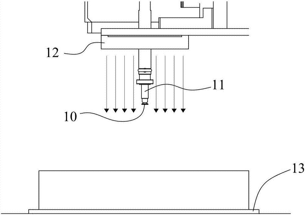
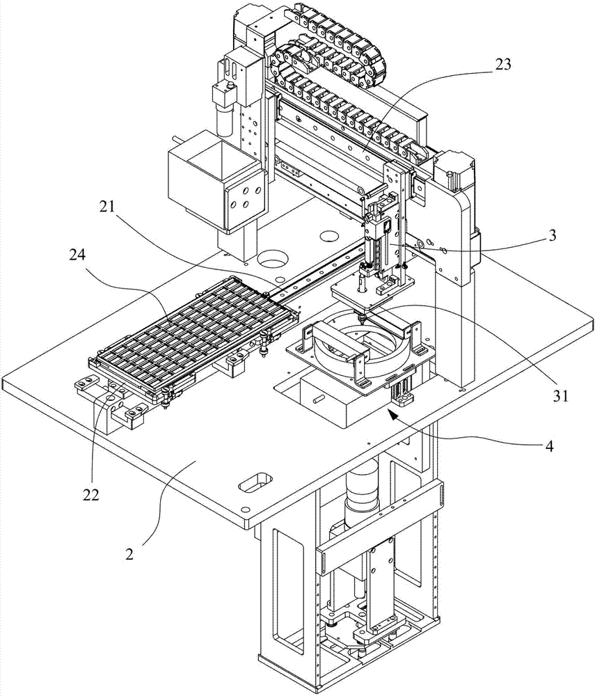
[0037] Such as image 3 Shown is a perspective view of the semiconductor component appearance inspection equipment of the present invention. The appearance inspection equipment of the semiconductor component of the present invention is that a transfer track 21, a carrier 22, a traverse track 23, a pick-and-place mechanism 3 and an appearance inspection area 4 are installed on the base 2, and the carrier 22 is installed on the mobile On the loading track 21, a carrier plate 24 can be carried for linear movement in the first direction, wherein the carrier plate 24 is used to place the semiconductor components to be tested; , the pick-and-place mechanism 3 is installed on the traversing track 23 and can move in a second direction, w...


PUM


Abstract

The invention provides an appearance inspection apparatus for a semiconductor assembly, and an optical path structure thereof. A base of the optical path structure is at least provided with a pickingand placing mechanism and an appearance inspection zone, wherein the picking and placing mechanism is provided with a suction head; the suction head comprises, from top to bottom, a buckling and clamping sleeve member, an annular sleeve and a suction nozzle; the annular sleeve has a conical surface which is increasing smaller from top to bottom; and the appearance inspection zone at least comprises two sets of strip light source, and the two sets of strip light source are apart from each other and arranged face to face. Thus, when the suction head is moved to a place located between the two sets of strip light source, light emitted by the two sets of strip light source is downwardly reflected by the conical surface of the annular sleeve, so uniform backlight is provided for inspection.

Description

technical field [0001] The invention belongs to the technical field of semiconductor component appearance inspection equipment, and in particular relates to a semiconductor component appearance inspection equipment and an optical path structure that can improve the backlight intensity in inspection operations and increase the accuracy of appearance inspection. Background technique [0002] With the development of science and technology, the size of semiconductor components is getting smaller and smaller to meet the needs of consumers who require products to be thin, light and short. After the semiconductor components are produced, they will be placed on the carrier tray, and then moved to the relevant inspection machine by the transfer mechanism for a series of inspection operations. As the size of the semiconductor components becomes smaller, relative derivative problems must be overcome in the inspection operations. [0003] figure 1 It is a structural schematic diagram o...

Claims


Application Information

Patent Timeline
IPC IPC(8): G01N21/01G01N21/95
CPCG01N21/01G01N21/95G01N2021/0112G01N2021/015
Inventor 詹勋亮梁居平傅书贤王柏谚李柏勋
Owner KING YUAN ELECTRONICS
Why Eureka
Try Eureka