
A Coarse Polishing Process for Reducing the Overall Flatness of Gallium Arsenide Double Polishing Chips

A gallium arsenide and flatness technology, applied in semiconductor/solid-state device manufacturing, electrical components, circuits, etc., can solve the problems of constant removal rate, increased flatness of double-polishing gallium arsenide wafers, etc., to reduce polishing pressure Effect

Active Publication Date: 2019-09-03
CHINA ELECTRONICS TECH GRP NO 46 RES INST
View PDF4 Cites 0 Cited by
  • Summary
  • Abstract
  • Description
  • Claims
  • Application Information

AI Technical Summary

Problems solved by technology

Different from single-sided chemical mechanical polishing, in the process of double-sided chemical mechanical polishing, the front and back of gallium arsenide double-throwing wafers are removed at the same time. At present, the commonly used polishing time is 890s, and the polishing pressure is 6kg per piece. The polishing cloth model is SUBAⅣ or SUBAⅩ, the speed of the polishing disc is 45rpm, the speed of the inner ring gear is 35rpm, the speed of the outer ring gear is 25rpm, and the speed of the inner and outer ring gears is operated at a ratio of 1.4:1. Finally, a product with a standard thickness was obtained, but due to the fast speed and the fast removal rate on the surface, the running track of the gallium arsenide double throwing disc was mainly concentrated in the center area of ​​the polishing cloth, and the loss in the center area of ​​the polishing cloth was greater than the edge loss during the polishing process of 890s , so in the subsequent processing process, the removal rate of the center of the GaAs double-throw wafer will decrease, while the removal rate of the edge will remain unchanged, which will cause the center of the GaAs double-throw wafer to be thicker than the edge, and thus make the GaAs double-throw wafer The overall flatness is increased, so the current process is difficult to ensure the overall flatness while ensuring the surface quality of the throwing plate. Usually, the overall flatness can only be guaranteed at 3 µm, and the maximum local flatness per 4 square microns is basically 2.5-3 µm. The average value can only guarantee 2µm

Method used


Image

  • A Coarse Polishing Process for Reducing the Overall Flatness of Gallium Arsenide Double Polishing Chips
  • A Coarse Polishing Process for Reducing the Overall Flatness of Gallium Arsenide Double Polishing Chips
  • A Coarse Polishing Process for Reducing the Overall Flatness of Gallium Arsenide Double Polishing Chips

Examples


Embodiment 1

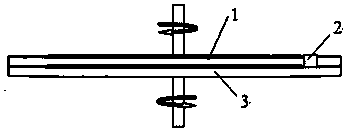
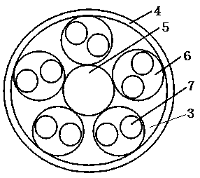
[0025] Embodiment 1: A rough polishing process for reducing the overall flatness of gallium arsenide double-throwing wafers is carried out according to the following steps:

[0026] In the first step, GaAs double-throwing wafers are sorted by 7 thicknesses, the sorting thickness is 700±5µm, every group of 10 pieces, and the thickness difference is less than or equal to 3µm.

[0027] In the second step, weigh 15L of deionized water with a 5L measuring cup and pour it into a clean coarse liquid throwing bucket, use a 1000ml measuring cup to weigh 600ml of NaClO solution and pour it into 15L of deionized water, stir the glass rod clockwise for 10 laps, and then weigh it with a 1000ml measuring cup Amount of 800ml containing SiO with a particle size of 85µm 2 The particle solution was poured into the previously prepared solution, and the glass rod was stirred clockwise for 10 laps.

[0028] The third step is to put an epoxy resin planetary wheel 6 on the surface of the lower poli...

Embodiment 2

[0042] Example 2: The difference between this embodiment and Example 1 is: Step 2: 800ml NaClO solution, 1000ml containing SiO with a particle size of 85µm 2 Particle solution, other steps and parameters are the same as in Example 1.

Embodiment 3

[0043] Embodiment 3: The difference between this embodiment and Embodiment 1 is: in step 5, the liquid application pipe 2 sends a rough throwing liquid flow rate of 7.0ml / s, the third stage rough throwing time is 900s, the pressure is 50kg, and the pressurization time is 30s. The rotation speed of the ring gear 5 is 15 rpm, the rotation speed of the outer ring gear 4 is 25 rpm, and the rotation speed of the lower polishing disc 3 is 35 rpm. Other steps and parameters are the same as those in the first embodiment.


PUM


Abstract

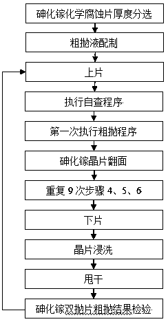
The invention discloses a rough polishing process for reducing the overall flatness of the gallium arsenide double-polished sheet, which comprises the following steps: after a rough polishing solutionis prepared, uniformly placing epoxy resin planetary wheels on a polishing disk surface; then, upwards placing the front side of the gallium arsenide double-polished sheet with the thickness deviation of 3 [mu] m in the hole of the epoxy resin planetary wheel; executing a self-checking program; checking the self-spinning conditions of the epoxy resin planetary wheels and the gallium arsenide double-polished sheet; after the self-checking program is executed, descending the upper polishing disc to finish execution of the rough polishing program for the first time; after the first rough polishing program is finished, turning over the gallium arsenide double-polished sheet; placing the back side of the double-polished sheet upwards and executing the self-checking program; then, executing therough polishing program for the second time; after ten times of operation are repeated, taking out the gallium arsenide double-polished sheet from the epoxy resin planetary wheels; and putting into awhite basket for cleaning and spin-drying. According to the embodiment of the invention, the overall flatness of the gallium arsenide double-polished sheet is effectively improved.

Description

technical field [0001] The invention relates to a rough polishing process for reducing the overall flatness of a gallium arsenide double-throwing sheet, belongs to the technical field of semiconductor material preparation, and is suitable for a double-sided rough polishing method used in the preparation process of a gallium arsenide double-throwing sheet. Background technique [0002] With the development of semiconductor integrated circuits, the diameter of gallium arsenide double throw wafers gradually increases. Although small-diameter GaAs double-polishing wafers are still processed by single-side polishing, in order to pursue better polishing quality, double-side polishing has gradually become the main processing technology for large-diameter GaAs double-polishing wafers. However, the reduction of the electronic characteristic line width and the improvement of the integration level put forward higher requirements for the uniformity of removal on-chip of GaAs double-thro...

Claims


Application Information

Patent Timeline
Patent Type & Authority Patents(China)
IPC IPC(8): H01L21/304H01L21/306
Inventor 李穆朗郭明孙强
Owner CHINA ELECTRONICS TECH GRP NO 46 RES INST
Learn More